


Content last revised on September 12, 2026
Benchtop Waveform Tuning: Mitigating Stress via Symmetrical Busbar Geometry for High-Current K200A02
| Model | K200A02 |
|---|---|
| Manufacturer | Vincotech |
| Category | IGBT Module |
| Package | Module |
| Topology | General Power Stage |
| Series | Standard |
| Voltage and Current Ratings | Not specified in the supplied official product data |
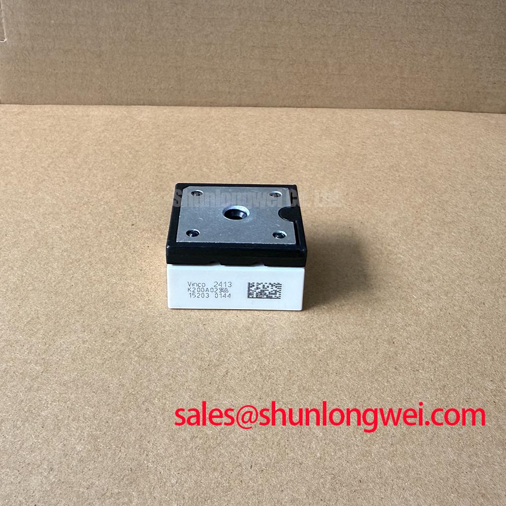
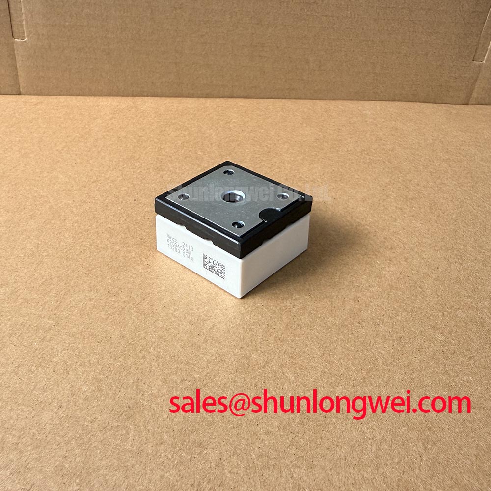
Probe each main-terminal path and gate-drive return path with power removed, then compare resistance continuity and physical conductor length between parallel switching positions before connecting the DC link. The K200A02 is identified as a Vincotech IGBT Module with a general power-stage topology, so its terminal function and permissible operating conditions must be matched to the original equipment schematic and module documentation.
Unequal busbar routing can create different commutation-loop inductance between otherwise similar switching paths. On an oscilloscope, this often appears as unequal collector-emitter overshoot, ringing frequency, or turn-off transition shape. Measure each waveform with the same probe method and grounding arrangement. A different trace does not establish a single cause, but it can direct inspection toward busbar symmetry, gate-loop routing, driver reference integrity, or DC-link capacitor placement.
Temperature dependence of collector-emitter saturation voltage is commonly considered during IGBT current-sharing analysis. This is a Design Consideration, not an official K200A02 performance claim: if parallel devices are operating under comparable thermal and drive conditions, the temperature characteristic can support steadier static current distribution. Dynamic sharing remains dependent on matched gate wiring, driver timing, parasitic inductance, and the surrounding switching network.
Keep the outgoing gate conductor and its return conductor close together, and prevent one gate path from crossing the high-current commutation loop of another path. Where a commercial string inverter or micro-grid energy-storage converter uses parallel power positions, engineers should capture turn-on and turn-off waveforms at equivalent operating conditions and compare them against the equipment’s known-good channel.
A related power-stage candidate, P084A2004, can be reviewed only through a full schematic, terminal-layout, electrical-rating, thermal-interface, and gate-driver compatibility assessment. Matching an overall package category alone does not establish electrical interchangeability.
💡 Bench Tip: Discharge the DC link, use ESD controls at gate terminals, and record cold-state diode-mode readings from a known-good assembly before judging a removed module.
K200A02 Circuit Protection & Reliability: Calibrating Junction-to-Case Thermal Network Simulation
Capture pulse width, repetition pattern, case temperature, and current waveform from the actual converter before estimating thermal stress during a suspected overload event. A junction-to-case thermal model is useful only when its model data, mounting condition, heat-sink interface, and real switching losses correspond to the installed power stage. No junction-to-case thermal impedance, maximum junction temperature, or overload rating is specified in the supplied official K200A02 data.
For pulsed loading, engineers commonly use a multi-section RC thermal network to represent the delayed flow of heat from junction to case. This is an Engineering Calculation when manufacturer thermal-network values and measured loss inputs are available. The calculated peak junction temperature must then be checked against the applicable manufacturer limit for the exact module and operating condition.
Gate interlock behavior deserves equal attention. Monitor the complementary gate commands at the module-side driver connection, rather than only at a controller output. A shoot-through signature may arise from timing overlap, a disturbed driver supply, excessive common-mode reference movement, or an incorrect return path. Dead time is a system-determined setting: it must prevent simultaneous conduction while preserving the waveform and efficiency requirements demonstrated in switching tests.
Negative gate bias and gate-emitter clamping are also system-level Design Considerations. Their suitability depends on the installed driver architecture and the voltage limits documented for the selected module. Avoid assuming a drive-voltage value from another IGBT family, even where the mechanical package looks familiar.
In converters with a rectification or complementary power section, the relationship between the switching module, DC-link capacitors, and associated devices must be traced through the actual schematic. The MMG75S170B is relevant for neutral review where a separate rectifier or companion stage is under evaluation; it is not presented as a direct substitute for K200A02.
For industrial energy-storage and inverter repairs, thermal-paste coverage, heat-sink flatness, clamp condition, and airflow should be inspected alongside electrical measurements. These installation factors can alter case-temperature behavior without proving a defect within the module itself.
Assembly Integrity & Layout Architecture: Implementing High-Speed Fault Management with VCE Desaturation for K200A02
Check the desaturation sensing route from the driver to the collector-side sensing point for damaged insulation, loose joints, contamination, and coupling to noisy switching conductors. Desaturation protection is commonly used to detect an abnormal rise in collector-emitter voltage while a gate command is active. Its threshold, blanking arrangement, and reaction time belong to the gate-driver and complete converter design, not to the supplied K200A02 product facts.
A valid fault test requires an approved controlled test arrangement and a waveform capture at the device-side gate and collector-emitter nodes. If a protection event causes a severe voltage excursion, inspect the physical location of the sensing network, gate-return path, DC-link loop, and clamp arrangement. The result may indicate layout coupling, unsuitable fault-turn-off behavior, gate-driver malfunction, or another issue in the surrounding circuit; it should not be reduced to a single-cause diagnosis.
Two-stage soft turn-off is a common Design Consideration for limiting inductive overvoltage during abnormal current interruption. The appropriate gate-current profile depends on the driver, the power-loop inductance, the DC-link voltage, the connected load, and the switching safe-operating information for the exact device. System engineers should validate peak voltage and current margins using captured fault waveforms.
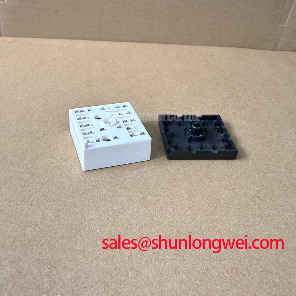
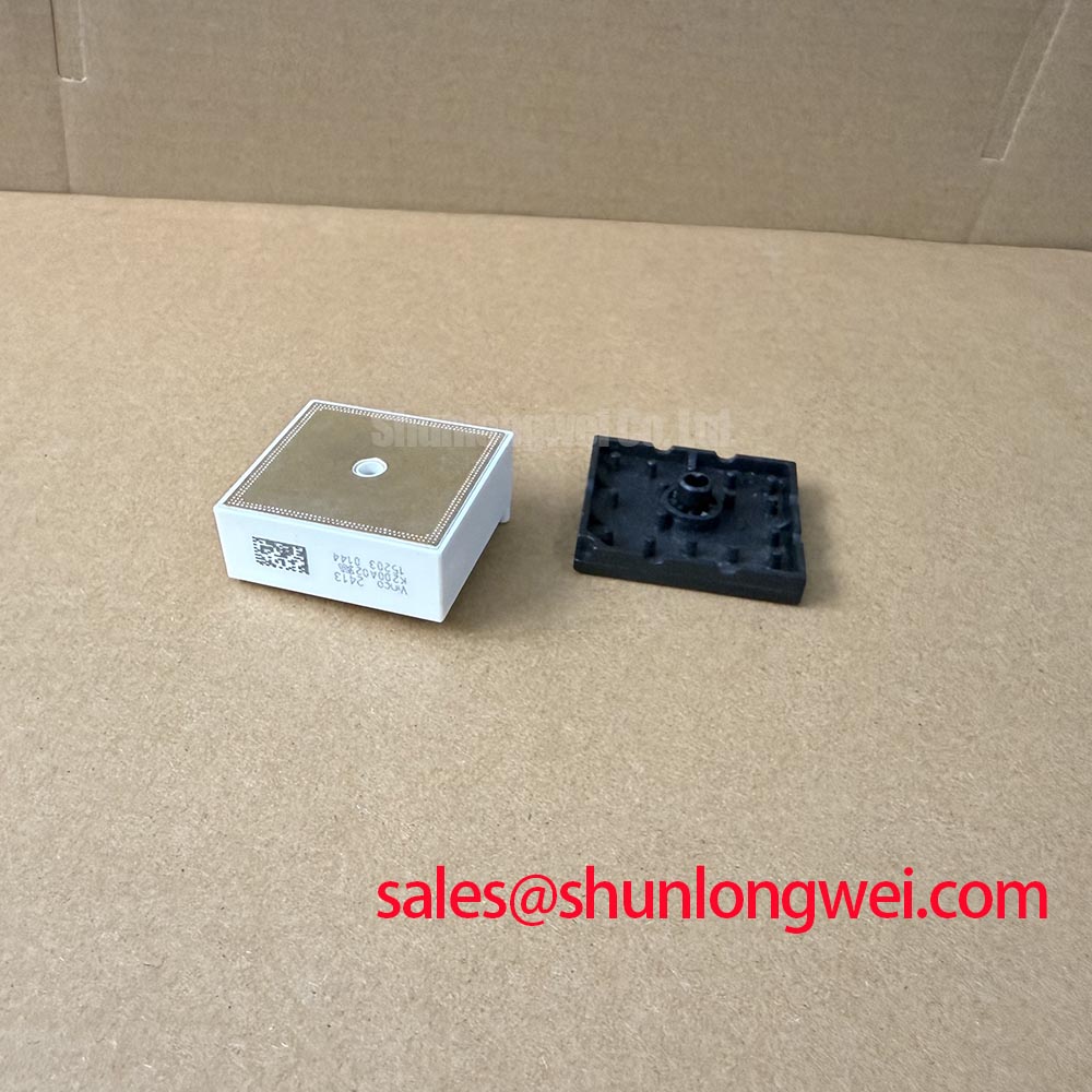
Mechanical assembly checks should include terminal alignment, insulated clearances required by the host equipment, heat-sink contact quality, and gate-connector seating. Do not force a module into a misaligned busbar stack. Mechanical stress at a terminal can impair connection integrity and distort later diagnostic measurements.
The switching behavior behind desaturation monitoring follows the same broad IGBT conduction and gate-control principles described in this external reference on Insulated-Gate Bipolar Transistor physics and operation. Device-level voltage and current limits, however, must come from the applicable K200A02 manufacturer documentation rather than from general IGBT theory.
Benchtop Waveform Tuning: Mitigating Stress via DC-Link Capacitance Bank Layout and Low-ESR Paths for K200A02
Measure collector-emitter overshoot at the module terminals with a low-inductance probing method, then compare the result while inspecting the distance and conductor geometry between the DC-link capacitor bank and the power module. During turn-off, peak voltage follows the general relationship of DC-link voltage plus the voltage generated by loop inductance and changing current. This is an Engineering Calculation only when the actual loop inductance and current-transition data have been measured or credibly modeled.
Place the high-frequency DC-link path so that outgoing and return current conductors remain closely coupled. Symmetrical planar busbar geometry can reduce loop area and make parallel switching paths more consistent. The final layout target is system-determined and must be verified against switching waveforms, DC-link voltage, load current, and the applicable voltage limit for the exact K200A02 installation.
Inspect capacitor-bank connections for looseness, corrosion, heat discoloration, or uneven current-path geometry. Capacitor degradation, a long laminated-busbar path, an unsuitable snubber connection, or probe-induced ringing can all affect observed waveforms. Compare measurements under repeatable operating states and use a known-good channel where the equipment provides one.
Regenerative braking and energy-storage transitions can move substantial energy through the DC link. The braking chopper, brake resistor, battery interface, control logic, and inverter power stage must be evaluated as a combined system. A braking resistor’s energy capability and a snubber network’s value cannot be assigned from the K200A02 package designation alone.
For broader context on how SiC and GaN technologies differ from conventional silicon power-switching approaches, see Wide Bandgap Revolution. That technical background does not establish a change in the K200A02 module’s supplied specifications or its compatibility with a particular inverter design.