




Content last revised on October 28, 2026
Field Diagnostics & Commissioning: Main Power Terminal Contact Resistance in MC0500-16IO1 Topologies
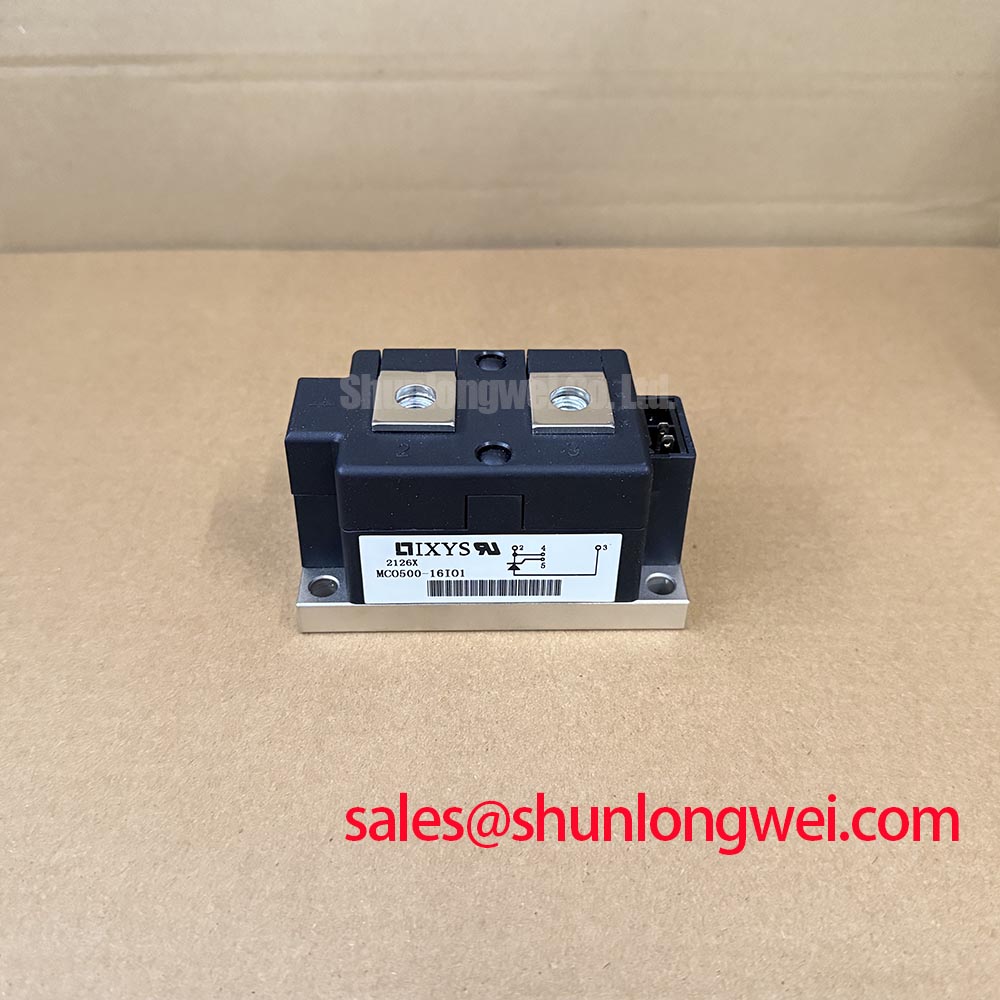
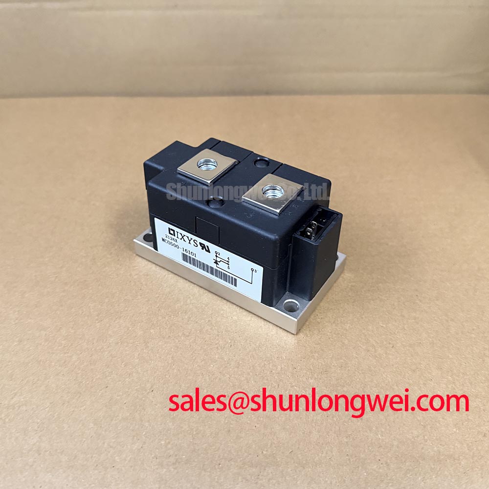
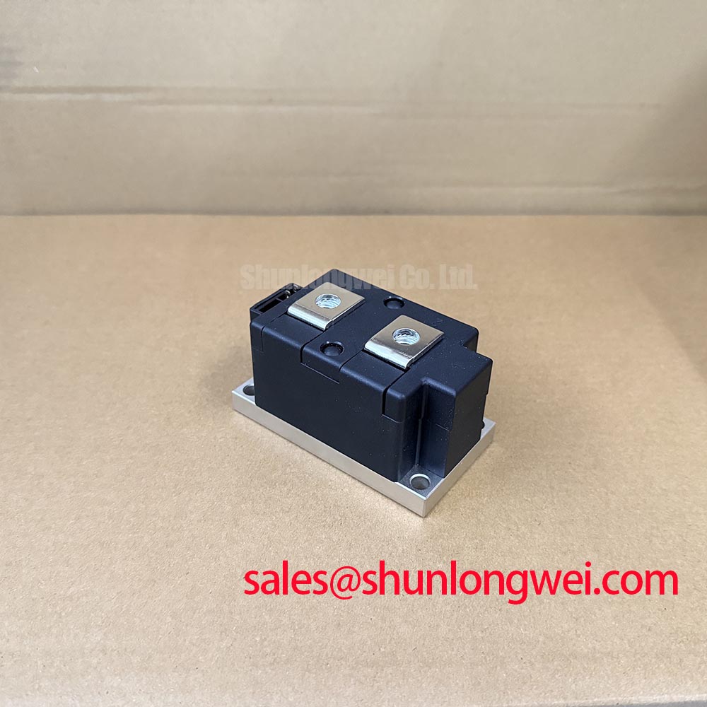
I isolate the power circuit, verify discharge, and position four-wire micro-ohmmeter probes across each bolted terminal joint before investigating localized heating. For the MC0500-16IO1 module, distinguish joint resistance from resistance through the semiconductor: probe placement must exclude unintended parallel paths and should remain consistent between comparative measurements.
Design Consideration: compare equivalent connections at comparable temperatures rather than imposing an unsupported universal contact-resistance limit. Record joint condition, conductor alignment, and the fastening procedure alongside each reading. A low cold resistance does not establish satisfactory performance under load; thermographic inspection during controlled commissioning can reveal uneven heating that warrants investigation of contact pressure, conductor loading, or nearby heat sources.
Keep attached conductors mechanically supported so their weight does not distort the terminal interface. Preserve electrical clearances using the equipment insulation requirements and actual conductor geometry. Tightening torque belongs to the specified terminal hardware and assembly instructions, not a generic module value. Where terminal heating persists, inspect both mating surfaces and the current path before attributing the temperature rise to an internal device fault.
MC0500-16IO1 Circuit Protection & Reliability: Calibrating Negative Gate Bias vs Active Miller Clamping
Establish the semiconductor type and gate-terminal function before evaluating negative bias or active Miller clamping. These techniques concern compatible insulated-gate switching devices; they are not interchangeable with the gate-drive requirements of a thyristor. Neither an IGBT topology nor an active-clamp requirement is established by the supplied MC0500-16IO1 specifications.
Design Consideration: where an insulated-gate topology is confirmed, evaluate off-state gate disturbance at the device terminals during commutation. Reverse-transfer capacitance couples switching-node transients into the gate circuit, while shared return-path inductance can distort the measured gate voltage. Gate charge and capacitance are different quantities; a capacitance entry alone does not establish the clamp current required throughout a switching transition.
An appropriate driver evaluation compares local gate waveforms, return routing, clamp timing, and permitted gate-voltage limits. Negative bias is a system-dependent option, not a default prescription. Where a freewheeling diode exists in the circuit, its reverse-recovery behavior can contribute to ringing and emissions; investigate the commutation waveform before selecting damping. The IGBT Design & Integration guide provides broader context for confirmed IGBT implementations, without establishing this module’s device technology.
MC0500-16IO1 Thermal-Electrical Optimization: Derating Guidelines and Practical Tuning
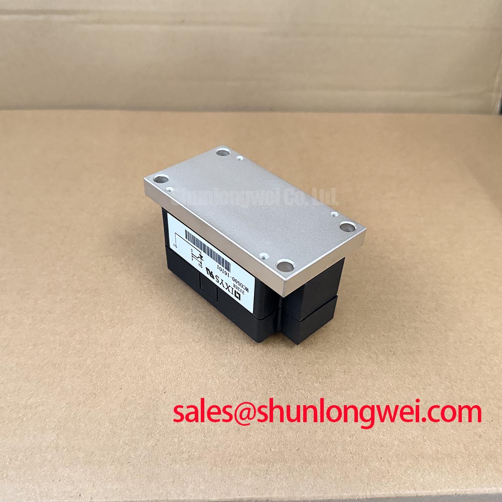
Inspect the mounting interface for flatness, contamination, and uneven thermal-interface coverage before assigning an operating-current limit. Design Consideration: the allowable electrical loading depends on device losses, cooling performance, interface resistance, and operating conditions. Use the applicable thermal-resistance definitions and temperature limits rather than treating a nominal current designation as a continuous assembly rating.
For a documented baseplate mounting arrangement, follow its specified thermal-interface material application and fastening sequence. Excess material can impair contact consistency, while uneven tightening can introduce mechanical stress. Do not apply pressure-contact spring calibration, double-sided cooling procedures, or package-specific torque values unless the mechanical drawing establishes that construction.
For parallel switching arrangements, establish temperature-dependent conduction behavior before relying on static current sharing. A positive on-state voltage temperature coefficient must not be assumed for MC0500-16IO1. Dynamic sharing additionally depends on branch impedance and switching behavior. Packaging concepts described in flip-chip interconnection illustrate why construction affects parasitics, but do not identify this module’s internal assembly. Potential evaluation for electric material-handling or forklift low-voltage traction equipment requires matching the actual topology, control interface, mechanical envelope, and electrical ratings.
Preventing Spurious Faults: Turn-Off di/dt Induced V_peak Clamping and Guidelines for MC0500-16IO1
Measure switching-node overshoot with an appropriately rated probe and a controlled measurement loop before selecting an absorption network. Engineering Calculation: the simplified relationship V_peak = V_DC + L_sigma × |di/dt| estimates the inductive contribution to peak voltage; actual ringing also depends on distributed capacitance, device behavior, and measurement placement.
Practical design tip: keep outgoing and return power paths closely coupled and geometrically balanced, then verify transient voltage margin during controlled switching tests appropriate to the confirmed device topology.
Design Consideration: select snubbers from measured transient energy, repetitive dissipation, and component pulse capability. If an MOV is considered, coordinate its clamping characteristic and repetitive-energy capability with the protected circuit. Semiconductor fuses serve a different protective function; Mersen semiconductor protection resources provide manufacturer guidance for assessing fuse characteristics against circuit requirements. After any protection change, repeat waveform measurements at the module terminals and inspect absorber temperature under representative duty.