


Content last revised on September 29, 2026
Transient Dynamics and Electrical Design for Short Circuit Protection
| Item | Official Product Information |
|---|---|
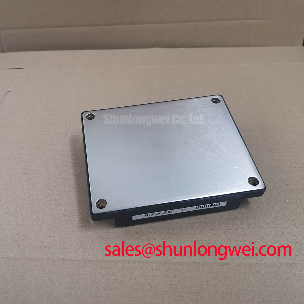
| Manufacturer | Toshiba |
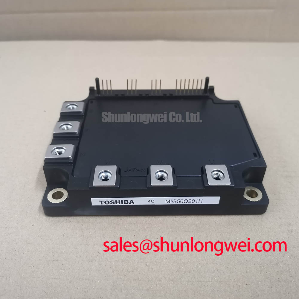
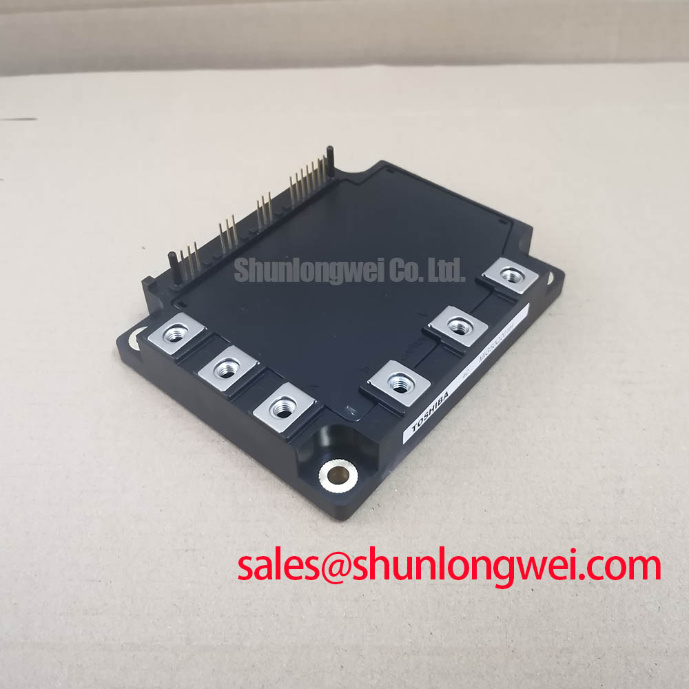
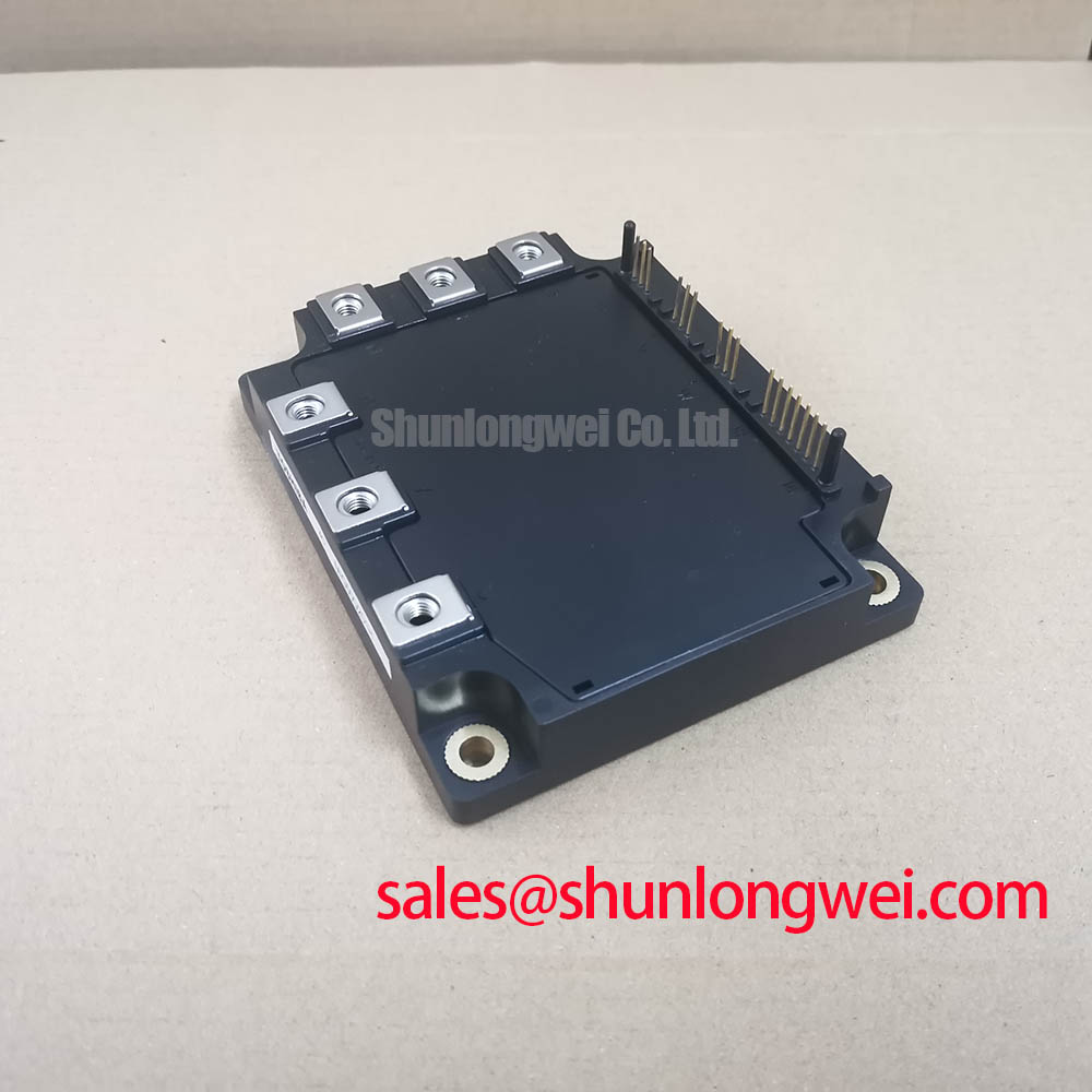
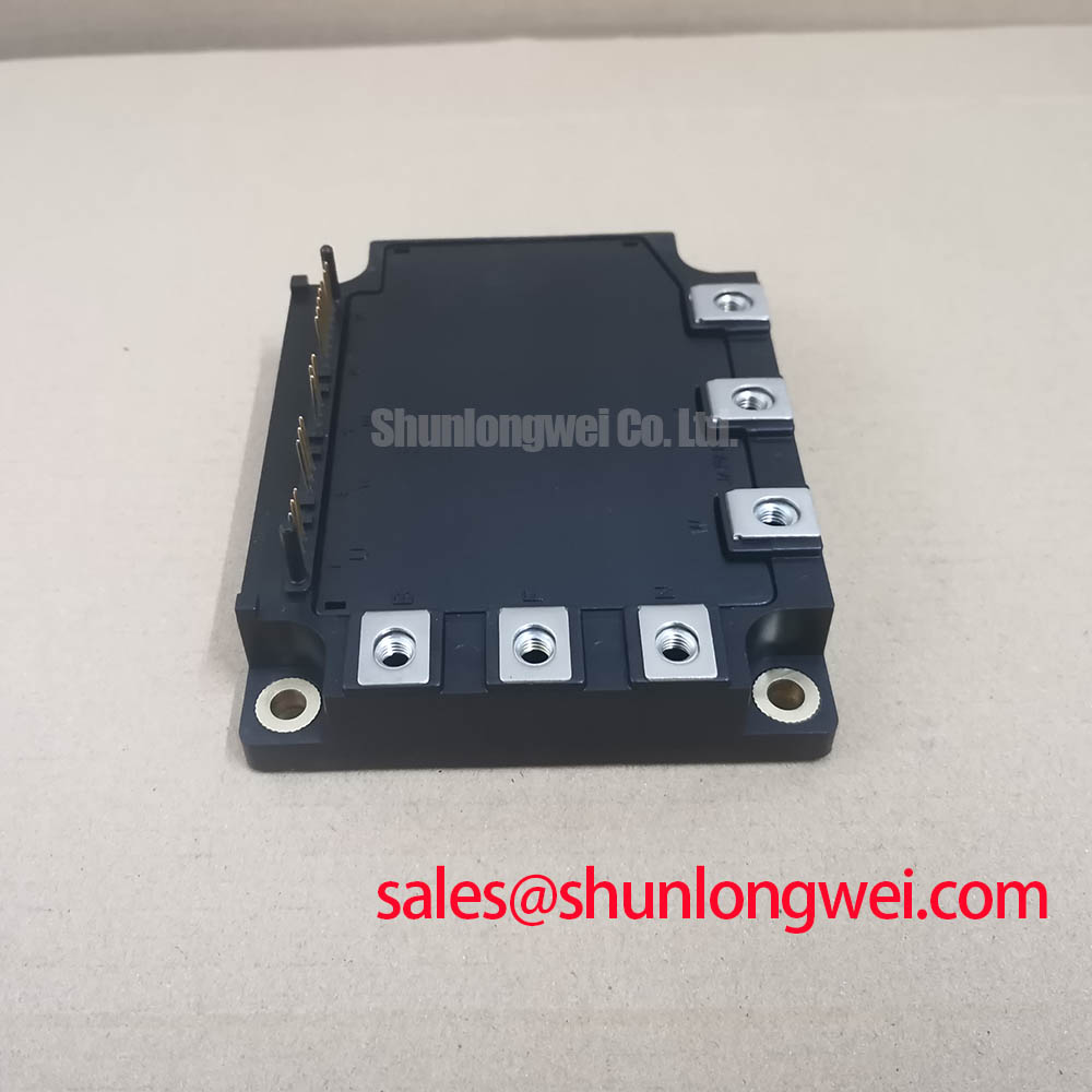
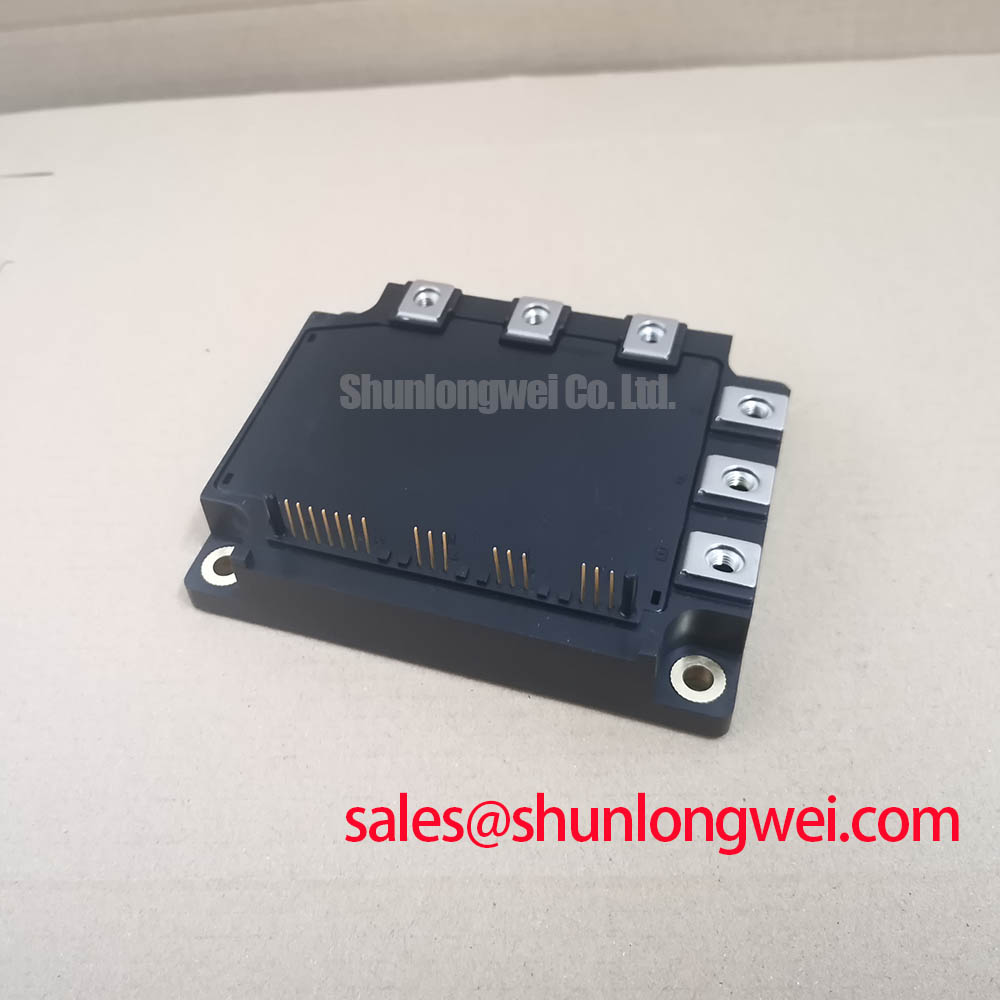
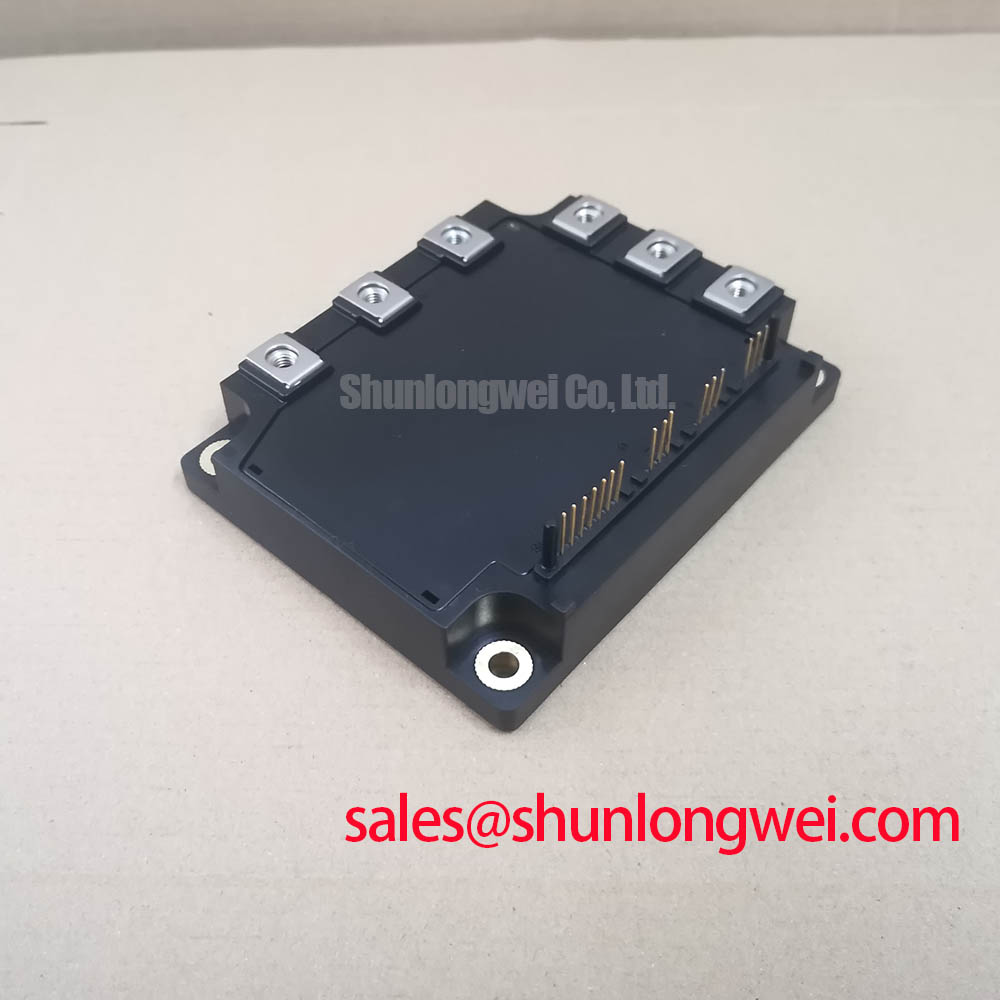
| Model | MIG50Q201H |
| Product category | Intelligent Power Module |
| Operating voltage | Standard Industrial Rating |
| Operating current | Standard Operating Current |
| Package and technology | Toshiba Intelligent Power Module |
Probe the gate command, collector emitter voltage, and current feedback together when a protection trip occurs on MIG50Q201H, then compare the captured sequence with a known good switching cycle before changing the gate network.
The supplied product information identifies this device as a Toshiba Intelligent Power Module with a standard industrial voltage rating and standard operating current classification. It does not provide a numerical collector emitter voltage, continuous collector current, short circuit withstand time, or SCSOA curve. Those values must therefore be taken from the original Toshiba documentation applicable to the exact production variant before a protection threshold is selected.
For a commercial string inverter or microgrid energy storage inverter, short circuit protection normally combines current sensing, desaturation or voltage monitoring, gate control, and a hardware shutdown path. A design evaluation may target detection within the system protection interval, including a sub 10 microsecond assessment where the switching energy and module short circuit capability make that interval relevant. This is a design target for the surrounding inverter, not an official rating assigned here to the module.
During bench testing, place the current probe so that it measures the complete commutation path rather than only a local branch. Trigger on the protection signal and inspect whether the gate voltage collapses before the collector emitter voltage develops a damaging overshoot. A trip that appears late may involve sensor propagation delay, filtering, controller latency, driver saturation, or common mode interference. The waveform should be reviewed as a complete time sequence rather than attributed to one component without evidence.
A two stage soft turn off strategy can be evaluated when a direct gate collapse produces excessive inductive voltage. The first stage reduces the gate drive current under fault conditions, while the second stage completes turn off after the main current has begun to fall. The exact gate resistance, timing, clamp level, and driver current are system determined. Designers should verify the resulting peak voltage against the documented module limit and the DC link operating envelope during worst case switching tests.
Keep the fault detection loop physically separate from high di per dt power paths. The current sensor return, driver reference, and protection comparator reference should have controlled return paths so that a power return transient does not resemble a short circuit or suppress a genuine fault. Clearance and creepage around the DC link and switching nodes must be selected according to the working voltage, pollution environment, insulation system, and applicable equipment standard.
When the inverter includes a regenerative braking chopper or a large braking resistor, test the transition from energy absorption to fault shutdown separately from normal motor regeneration. A braking resistor can keep the DC link elevated while the protection circuit is already reducing gate drive. The oscilloscope record should include DC link voltage, chopper current, gate command, and fault status so that the energy path remains visible.
The neutral comparison point for this work is the Toshiba device documentation and the actual inverter reference design. The general IPM protection principles described by Infineon CIPOS Intelligent Power Modules are useful for understanding integrated driver and protection functions, but they do not establish the electrical limits of Toshiba MIG50Q201H.
Benchtop Waveform Tuning and Transient Thermal Impedance
Record the collector current, switching duration, case temperature, and pulse repetition pattern while applying the intended overload waveform; do not infer junction temperature from case temperature alone.
Heavy pulsed overload creates a transient thermal problem because the semiconductor junction responds faster than the heat sink and mounting assembly. A transient thermal impedance model is commonly represented by several thermal resistance and time constant branches. The practical calculation uses the pulse power history and the applicable junction to case transient data from the manufacturer, then adds the case to heat sink and heat sink to ambient paths established by the actual assembly.
No numerical transient thermal impedance curve, junction temperature limit, thermal resistance, or overload pulse rating is provided in the supplied product context. The peak junction temperature therefore cannot be calculated defensibly from the information available here. A valid test requires the Toshiba thermal curves for this exact model, the installed interface material, the mounting condition, and the measured case temperature at the module reference point.
For regenerative braking, measure the energy absorbed by the resistor and the switching losses in the chopper independently. A resistor bank may tolerate a pulse that still produces unacceptable semiconductor junction heating if the switching frequency, current ripple, or turn off loss is higher than expected. The test sequence should include repeated pulses at the intended duty pattern, followed by a cooling interval representative of the real equipment cycle.
Gate driver power integrity also deserves a direct waveform check. Where a high side driver uses a bootstrap supply, the capacitor selection should account for gate charge, driver quiescent current, leakage, bootstrap diode behavior, switching frequency, duty cycle, startup behavior, and permitted voltage ripple. The required capacitance is a system calculation based on those loads and the driver operating limits. It cannot be assigned from the MIG50Q201H model name alone.
Use a differential probe for floating gate and power measurements, confirm probe bandwidth and common mode range, and compare the gate waveform at the module terminals with the waveform at the driver output. A large difference can indicate trace inductance, return path coupling, probe placement, driver supply droop, or an unsuitable gate network. The waveform should be checked at cold start and after the module and heat sink have reached the intended operating temperature.
Positive temperature coefficient behavior can assist static current sharing when multiple compatible switching devices are paralleled, but it does not guarantee dynamic sharing during turn on or turn off. Gate loop inductance, propagation mismatch, emitter path resistance, and thermal coupling must be evaluated as a complete design. Parallel operation should only be considered after the terminal configuration, electrical ratings, gate drive requirements, and manufacturer guidance for the exact module have been confirmed.
For comparison work, engineers may review the electrically related PM75CSD120 as a separate product record. It should not be treated as an automatic substitute for MIG50Q201H. Voltage class, current rating, internal topology, protection behavior, terminal arrangement, switching characteristics, and mechanical fit all require a documented comparison.
Bench Tip: Use ESD controls and record a cold state waveform and terminal resistance baseline before applying the first powered pulse.
Kelvin Emitter Connection and Gate Return Control
Measure the gate emitter voltage directly at the module terminals during the fastest current transition, then compare it with the driver reference to determine whether the observed oscillation belongs to the gate loop or the main power return.
A separate auxiliary emitter or Kelvin emitter connection can reduce the influence of high current emitter voltage drop on the gate driver reference, but the existence and function of such a terminal must be confirmed from the exact Toshiba terminal diagram. The supplied product context does not publish a pin assignment. Do not assume that a visually similar terminal is a Kelvin emitter, auxiliary emitter, or signal return.
If the terminal map confirms a dedicated gate return, route that return directly to the driver reference and keep it distinct from the main emitter current path. The main emitter connection must carry the intended load current with an impedance appropriate to the switching current. Joining the two returns at an uncontrolled point can reintroduce mutual coupling and make the gate voltage appear to move during commutation.
During troubleshooting, place one differential probe across gate and emitter at the module and another across the driver output reference. If the driver output is stable but the module gate emitter waveform contains ringing, inspect the gate loop, connector transition, auxiliary return, and local decoupling. If both waveforms move together, investigate driver supply bounce, controller ground movement, isolation capacitance, or measurement reference errors.
The same distinction matters for negative gate bias. A negative turn off bias may be considered in systems where Miller coupling or high dv per dt creates unwanted turn on risk, but its magnitude, timing, and suitability are controlled by the module and driver documentation. A negative supply should never be introduced solely because a switching waveform looks noisy. Verify the permitted gate emitter range, driver isolation behavior, and startup sequence first.
Common mode ground bounce can also corrupt current feedback and short circuit detection. Place signal conditioning components with a clear reference to the intended control return, maintain separation from the commutation loop, and validate the protection signal while the power stage is switching. Shielding can reduce capacitive coupling, but a shield connected at an unsuitable point can transfer switching current into the control reference.
Layout clearance must reflect the inverter DC link and switching node voltage rather than the nominal control supply. Creepage, clearance, slotting, insulation barriers, connector spacing, and probe access should be reviewed against the final enclosure and pollution conditions. These are design considerations for the complete converter and are not physical dimensions specified for MIG50Q201H in the supplied data.
In a rectifier and inverter assembly, the front end may use a separate device such as PM150DSA120 as an associated rectification stage. That relationship does not establish electrical compatibility. The rectifier output, DC link capacitor arrangement, precharge circuit, braking path, and IPM switching stage must be evaluated together.
Operational Boundaries for Altitude, SEB, and FIT Evaluation
When a converter operates above its original site altitude, log DC link voltage, switching temperature, cooling performance, insulation test results, and protection events at the actual installation location before assigning a derating decision.
Altitude can affect cooling, insulation coordination, and the electrical environment around high voltage conductors. Reduced air density may alter convective heat transfer and external insulation performance, while the power semiconductor itself is governed by its documented voltage, temperature, switching, and protection limits. An altitude adjustment cannot be derived from the MIG50Q201H model name or from a generic industrial classification.
Single Event Burnout and neutron related reliability require a qualified device reliability source, a defined terrestrial radiation environment, a voltage stress distribution, a mission profile, and an applicable calculation method. No Toshiba SEB cross section, neutron flux assumption, FIT model, altitude correction, or mission reliability dataset is provided in the supplied product context. A numerical FIT rate or failure probability would therefore be unsupported.
For an engineering review, collect the exact DC link maximum, switching overshoot, junction temperature estimate, altitude, operating hours, load profile, and fault history. Compare those conditions with the manufacturer’s rated voltage and safe operating information when available. The voltage headroom should be treated as a system verification item that includes parasitic inductance and measurement uncertainty. It should not be replaced by a universal percentage margin without a source.
Field troubleshooting should begin with non destructive checks. Inspect the power terminals, gate connector, heat sink interface, insulation barriers, and DC link discharge path. With the equipment isolated and discharged according to the site procedure, compare terminal behavior against a known good unit using an appropriate meter function. A diode test result or resistance reading can identify an asymmetry that deserves investigation, but it cannot by itself prove semiconductor health or establish a production limit.
For insulation verification, use the test voltage and duration specified by the equipment safety design and the applicable Toshiba documentation. The IPM should be disconnected or configured exactly as required by the test procedure because connected driver circuits, capacitors, sensors, and surge suppressors can change the result. Insulation resistance and dielectric withstand are different tests and should not be treated as interchangeable evidence.
Long duration operation should be evaluated through the complete thermal and electrical mission profile. Record cooling inlet conditions, case temperature, switching frequency, DC link behavior, protection trips, and load transitions. A single successful bench run does not establish a field lifetime, and no field failure rate or operating hour claim is made here.
For topology context, the discussion of Resonant Topologies in Home Appliances can help engineers compare commutation behavior across power conversion architectures. It does not define the ratings or reliability limits of this Toshiba IPM. Final integration decisions should remain tied to the original Toshiba documentation, measured waveforms, thermal results, and the applicable equipment standards.