


Content last revised on October 29, 2026
MIG75J6CSB1W Thermal-Electrical Optimization: Baseplate Thermal Grease Layer Control Practical Tuning
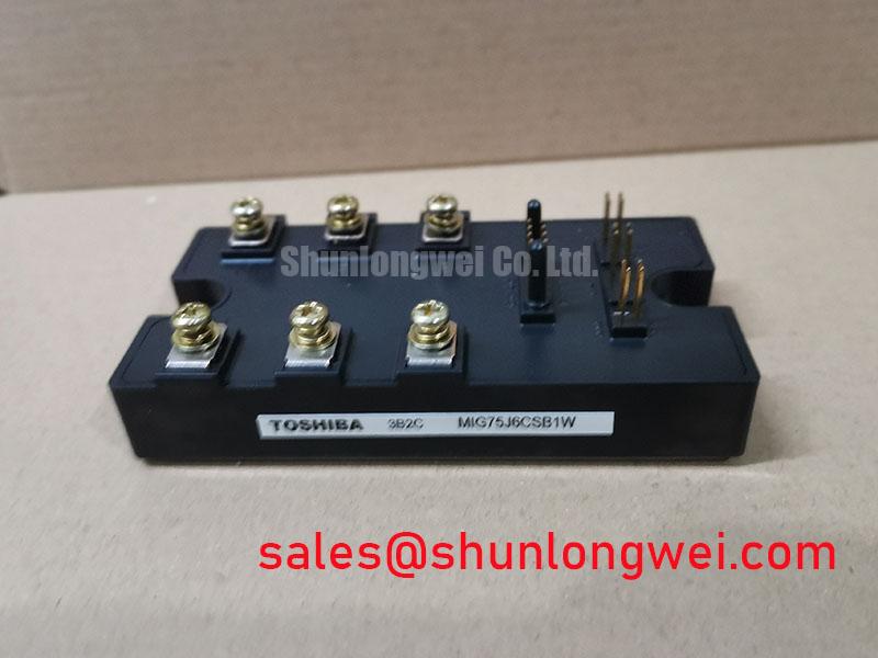
I inspect the heatsink contact surface and the module mounting face before applying fresh thermal compound, because an uneven contact pattern can undermine otherwise careful electrical testing. For the MIG75J6CSB1W, the relevant starting point is the actual assembly: retained compound, burrs around mounting holes, surface contamination, and evidence of uneven clamping. Inspect these features without scraping or altering the module contact surface.
Design Consideration: Thermal interface material should fill microscopic surface irregularities without becoming a thick spacer between the module and heatsink. Select its application method from the compound supplier’s instructions and the module assembly requirements. A generic grease thickness is not a Toshiba mounting specification. Where the maintenance procedure permits a contact-pattern inspection, examine transfer coverage for discontinuities and excessive squeeze-out before completing the installation.
Check heatsink flatness and mounting-face condition separately. Adding more grease is not a controlled remedy for significant curvature, damaged threads, or a distorted mounting surface. Bring the mounting screws into contact progressively, following the prescribed sequence and final torque for the assembly. Avoid pulling one corner fully down while the remaining mounting points are loose; the objective is even seating rather than forcing the package to follow an unsuitable surface.
Keep displaced compound away from terminal interfaces and preserve the equipment’s specified electrical clearances. After reassembly, compare temperature behavior under repeatable loading and cooling conditions. A temperature difference between otherwise similar operating states warrants checking airflow, contact coverage, current distribution, and measurement location rather than assigning the fault immediately to the module.
Before powered testing, I record cold terminal measurements using the documented circuit diagram. With external circuitry isolated as required by the service procedure, diode-mode measurements in both polarities can help compare corresponding current paths. Meter test current, temperature, and connected control circuitry influence the reading; a forward-voltage observation is not an independent acceptance limit for this part.
💡 Bench Tip: Discharge the DC link and verify its safe state before handling terminals, then use ESD precautions while comparing cold readings with a documented known-good reference.
For incoming inspection, keep power-terminal-to-baseplate insulation testing separate from diode checks. The 600.0 V electrical rating is not an insulation test voltage. Use the manufacturer’s specified terminal grouping, test voltage, duration, and acceptance criteria, together with the equipment maintenance procedure; an improvised withstand test can stress connected electronics without establishing useful insulation margin.
Benchtop Waveform Tuning: Assessing Diode Recovery Stress on MIG75J6CSB1W
Capture the commutating current and the associated switching-node voltage together before changing damping components. Design Consideration: In an IGBT bridge with antiparallel freewheeling paths, reverse recovery can contribute to turn-on current peaks and ringing. The peak reverse-recovery current, commonly written I_rrm, must be interpreted alongside commutation rate, junction temperature, bus conditions, and probe placement. A single peak on an oscilloscope does not establish the diode’s recovery softness.
Recovery softness describes the shape of the recovery waveform under defined conditions, and conventions for expressing it depend on the technical reference. An abrupt recovery tail can excite parasitic inductance and capacitance, but waveform shape must be distinguished from probe-loop pickup and current-sensor response before drawing conclusions.
Use suitably rated differential voltage measurement and a current probe appropriate to the event bandwidth. Keep the measurement geometry consistent between trials. If ringing changes substantially when the probe connection changes, resolve that measurement sensitivity before selecting a snubber. Compare the switching event at matched current and temperature so that a warmer diode or a different conduction interval is not mistaken for an improvement in damping.
Where the documented interface exposes an adjustable gate-drive path, turn-on resistance can influence commutation speed. For an intelligent power module, however, an external logic input is not automatically an accessible transistor gate. Any drive adjustment must respect the actual interface. An RC snubber is likewise a system-level option: determine its placement and component requirements from the measured oscillation, repetitive energy, and thermal loading rather than selecting values from the module’s current rating.
Separate switching-edge behavior from slower DC-link variation. In equipment using phase-angle-controlled upstream conversion, conduction angle can influence current pulses and bus ripple; it is not a diode-softness control. Similarly, ripple smoothing belongs to the DC-link design. Record the instantaneous bus condition during waveform comparisons so that changes in supply behavior are not attributed to the MIG75J6CSB1W.
When reviewing drive and supply coordination, the PM50RL1A060 can be examined as a separate power-module reference within a system bill-of-materials assessment, not assumed to be a front-end rectifier or a compatible companion. Its circuit arrangement and interface requirements require their own comparison.
The Infineon CIPOS™ Intelligent Power Modules (IPM) resource provides useful industry context for integrated power-module architectures. It does not establish Toshiba-specific recovery characteristics or electromagnetic compatibility. Any emission benefit from waveform tuning must be assessed at equipment level with the final wiring, enclosure, and operating conditions.
Benchtop Waveform Tuning: Mitigating Stress via Control Return Routing on MIG75J6CSB1W
Trace the control return against the power-current path before interpreting apparent gate noise. For IGBT terminology, the relevant transistor reference is the emitter, not the MOSFET source. Do not infer a separate Kelvin-emitter terminal from the module category or model name; use the Toshiba terminal drawing to identify the connections actually provided.
Design Consideration: Shared return-path inductance can generate a transient voltage when load current changes, disturbing the reference seen by a driver or control receiver. Where separate control and power returns are explicitly provided, route them according to the documented connection scheme. Keep outgoing control signals close to their intended returns and avoid sharing their return route with high-current commutation paths. Physical separation alone does not correct an incorrectly referenced interface.
For an external optocoupler or digital isolator, compare its common-mode transient immunity specification with the conditions at the isolation barrier. Evaluate polarity, supply conditions, pulse behavior, and the surrounding layout rather than treating the headline CMTI rating as a complete noise-immunity guarantee. Correlating an input command, receiver output, and switching-node transition can help distinguish a control-path disturbance from a genuine protection response.
If the host driver uses a bootstrap supply, inspect its voltage during the actual switching sequence and longest relevant high-side conduction interval. Charge replenishment depends on available recharge intervals, driver consumption, leakage, and the charging path. Check capacitor behavior and bootstrap-diode recovery against the external driver documentation. These are host-circuit considerations, not confirmed internal features of the Toshiba Intelligent Power Module.
The article Single-Supply Gate Drive for SiC MOSFETs offers background on gate-drive reference integrity and switching disturbances. Its SiC-specific bias strategies are not transferable settings for this Toshiba IPM. Apply only the general measurement and return-path principles that fit the documented interface.
For commercial string inverter or micro-grid energy-storage compatibility assessment, compare the bridge arrangement, control interface, cooling assembly, terminal positions, and protection coordination against the host design. During replacement-material review, the PM400DSA060 is a separate comparison candidate, not a confirmed substitute. Shared category terminology does not establish interchangeability.
Where the host equipment instead includes long motor leads, measure reflected-wave stress at the load as well as at the inverter terminals. Cable propagation and impedance discontinuities can produce different voltage peaks at those locations. Select any output reactor or filtering approach from the cable, motor, and drive requirements, then verify the resulting waveforms; a module-side snubber alone does not establish acceptable motor-terminal stress.