

Content last revised on September 27, 2026
Assembly Integrity and Gate Control for MZK400TS120
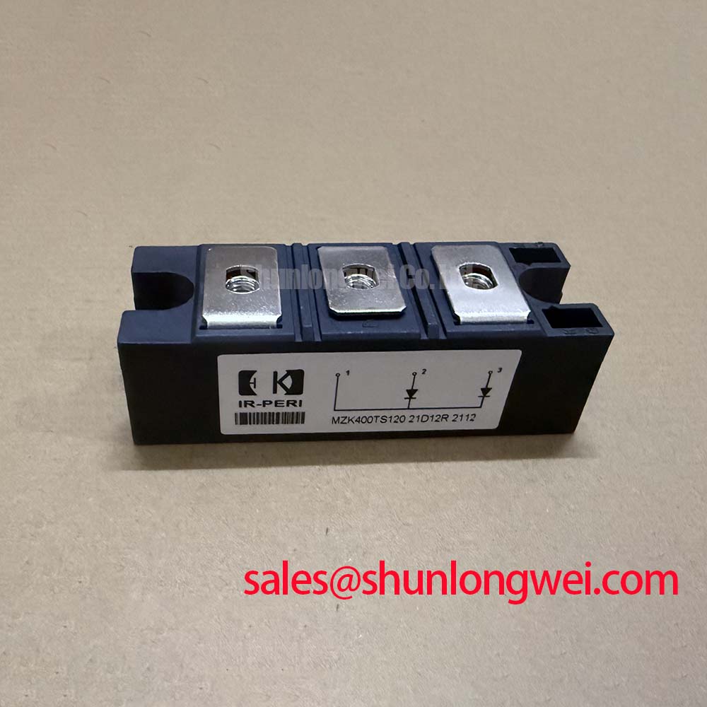
Before energizing a replacement, inspect the housing and terminals for mechanical damage, confirm the nameplate model, and record the cold-state impedance between the relevant power and gate terminals against a known-good unit. The Sanken MZK400TS120 is specified for high-power switching service, with a collector-emitter voltage rating of 1200 V, continuous collector current of 400 A at Tc = 80°C, total power dissipation of 1600 W at Tc = 25°C, and a maximum junction temperature of 150°C. These are official specification values supplied for product evaluation, not a complete system operating prescription.
| Parameter | Official Specification |
|---|---|
| Manufacturer | Sanken |
| Model | MZK400TS120 |
| Collector-emitter voltage, VCES | 1200 V |
| Continuous collector current, IC | 400 A at Tc = 80°C |
| Total power dissipation, Ptot | 1600 W at Tc = 25°C |
| Maximum junction temperature, Tjmax | 150°C |
| Product category | IGBT module |
When installing the MZK400TS120 in a commercial string inverter or micro-grid energy storage converter, begin with the original gate-drive schematic rather than assuming that another IGBT module uses the same pin arrangement or drive conditions. The published data supplied for this product confirms its main electrical and thermal ratings, but the system integrator should verify the complete terminal drawing, gate-emitter requirements, switching limits, internal topology, and any auxiliary terminal definitions from the applicable device documentation.
A high-voltage bridge can experience unwanted turn-on when the opposing switch sees a rapid collector-voltage transition. A negative gate bias or an active Miller clamp can be considered as part of the gate-drive architecture, but the permitted voltage range, clamp current, dead time, and protection thresholds must be established from the module data and tested in the actual converter. Do not transfer a negative-bias value from a different Sanken family or from a lower-current module without checking gate-emitter stress limits.
The practical layout objective is to keep the gate-drive return path separate from high-current commutation paths and to minimize the loop area around the gate resistor, driver output, module gate terminal, and emitter return. Where the module provides a dedicated auxiliary emitter or Kelvin-style connection, its use must be confirmed from the terminal drawing; it should not be inferred from the model designation. Gate traces should be routed away from the collector bus and switching node, with clearance and insulation selected according to the DC-link voltage, pollution environment, creepage requirement, and enclosure construction.
During a field replacement, use an oscilloscope with suitable isolated or differential probes to compare the gate-emitter waveform of the suspect leg with the corresponding healthy leg. Look for abnormal ringing, delayed turn-off, unequal propagation, or a gate waveform that changes when the power commutation node moves. These observations may indicate a drive-loop, grounding, isolation, or component-tolerance issue; they do not identify a failed module by themselves. Confirm the result with power removed, controlled resistance checks, and inspection of the driver supply and gate protection components.
⚠️ Field Alert: Disconnect the DC link and verify the discharge condition before removing gate-drive connectors or touching the module terminals.
Bench Waveform Tuning and Isolated Driver Coordination
Bench testing should separate gate-drive verification from high-energy bus testing. First confirm that the isolated driver supply starts correctly, remains stable during both turn-on and turn-off, and maintains the required galvanic isolation for the complete system. Isolation withstand, common-mode transient immunity, and driver timing are properties of the selected gate-driver power supply and control circuit, not official ratings of the MZK400TS120. Designers should verify them against the converter’s measured switching transients and the applicable safety design requirements.
For an inverter leg, the commutation loop includes the DC-link capacitor, busbar, module terminals, and the opposing switch or freewheeling path. Minimize parasitic loop inductance to reduce turn-off voltage overshoot, then verify the peak collector-emitter voltage with a properly compensated differential probe. A film snubber may be evaluated close to the commutation path when measured ringing shows that additional high-frequency energy control is required. Its capacitance, voltage rating, pulse-current capability, and loss must be selected from the switching waveform rather than copied from another assembly.
The freewheeling diode path deserves separate attention. Reverse-recovery softness, recovery charge, and the resulting current slope can influence voltage overshoot, conducted noise, and radiated EMI. The supplied product data does not provide a softness factor or recovery curve for the associated diode, so those values should be obtained from the relevant Sanken documentation or measured on the actual module. A spectrum change after a switching-frequency or gate-resistor adjustment can help locate a commutation problem, but it should be correlated with voltage and current probes before any component is condemned.
Do not treat a thyristor gate-trigger method as interchangeable with an IGBT gate-drive method. An IGBT requires controlled gate-emitter voltage, turn-off control, and protection against false triggering during high dv/dt events. If the converter uses pulse-train logic, desaturation protection, under-voltage lockout, or active Miller clamping, verify the timing relationship between these functions and the bridge dead time. A microsecond-scale delay may be significant in one topology and excessive in another, so the final setting remains system-determined.
The FP10R12KE3 can be reviewed as a related device in the upstream rectification or complementary power-stage context, but its ratings and control requirements must not be substituted for those of the MZK400TS120. In a service investigation, compare the full topology, voltage class, current path, protection scheme, and mechanical interface before considering any cross-reference.
Thermal Contact and Electrical Mounting Verification
The official thermal figures for the MZK400TS120 are 1600 W total power dissipation at Tc = 25°C and 150°C maximum junction temperature. They do not establish the heatsink size, allowable ambient temperature, switching frequency, overload duration, or permissible current in a finished inverter. Those values depend on conduction loss, switching loss, case temperature, airflow, coolant conditions where applicable, interface resistance, and the enclosure thermal path.
Before mounting, inspect the heatsink for burrs, contamination, local distortion, or a surface condition that could prevent uniform contact. Apply the selected thermal interface material as a consistent, thin layer according to its manufacturer’s process guidance. The purpose is to fill surface irregularities without creating a thick, uneven barrier. If the baseplate and heatsink do not sit naturally together, correct the mechanical cause rather than attempting to compensate with excessive fastening force.
Use the original mechanical drawing to verify hole pattern, washer arrangement, insulation hardware, and terminal clearance. Fasten progressively in a crosswise sequence when the mounting design calls for multiple screws, allowing the module base and heatsink to settle evenly. The correct torque is determined by the specified fastener, washer system, module construction, and manufacturer instructions; a generic torque value should not be presented as an MZK400TS120 factory parameter.
After assembly, inspect for squeezed-out interface material near insulated areas and confirm that the power terminals have not shifted under mechanical loading. Measure case temperature at a controlled operating point and compare the thermal gradient across the heatsink. An unexpected difference between parallel legs may arise from unequal current sharing, gate timing, busbar resistance, interface contact, or sensor placement. Use synchronized electrical and thermal measurements before changing the gate drive or reducing the load.
For potential use in commercial string inverters and micro-grid storage equipment, the system integrator should also verify enclosure airflow, service clearances, DC-link fault energy, fuse coordination, and insulation distances. The MZK400TS120 rating does not independently certify the complete inverter for EMC, safety, or grid-connection requirements.
Transient Thermal Impedance and Pulsed Overload Assessment
A short overload can produce a junction temperature rise that is not visible immediately at the module case. For this reason, a thermal assessment should use the manufacturer’s transient thermal impedance data when available, together with measured loss pulses and the actual cooling boundary. A multi-section RC thermal model can represent the junction-to-case response, but its constants must come from an authoritative thermal curve or validated test rather than being invented from the steady-state power rating.
Calculate the pulse loss from measured collector current, collector-emitter voltage, switching transitions, and conduction intervals. Then combine the resulting energy profile with the case-temperature waveform and the specified maximum junction temperature of 150°C. The important engineering check is whether the calculated peak junction temperature remains within the documented boundary during the complete pulse sequence, including repeated overloads and recovery intervals. If the datasheet does not provide the required transient curve, use conservative bench characterization and clearly document the assumptions.
Thermal sensors should be attached where they represent the module case rather than a nearby heatsink location. A heatsink sensor can lag the case during rapid power changes, while an infrared reading can be affected by surface emissivity and access angle. The Seebeck effect and temperature sensing principles are relevant when thermocouples are used, but sensor wiring and electrical isolation still need practical verification in a high dv/dt converter.
Long-duration reliability analysis should distinguish measured temperature cycling from a formal lifetime prediction. Without qualified mission-profile data, junction-temperature history, power-cycling parameters, and an applicable reliability model, do not assign a service-life value to this module. Engineers evaluating gate insulation stress can consult the general discussion of negative-bias temperature instability, while recognizing that a general mechanism reference is not a product-specific qualification result.
For a broader explanation of IGBT switching physics, thermal paths, and structural considerations, see The Ultimate IGBT Knowledge Base. When comparing a different power-stage option, the FS100R12N2T4 may be reviewed as a separate device, but voltage, current, package, gate-drive, thermal, and protection compatibility must be verified independently before any substitution is considered.