
Content last revised on September 12, 2026
Transient Dynamics & Electrical Design: Fault-Clearing Dynamics: Type-I/II Desatur on P840C4806
| Manufacturer | Vincotech |
|---|---|
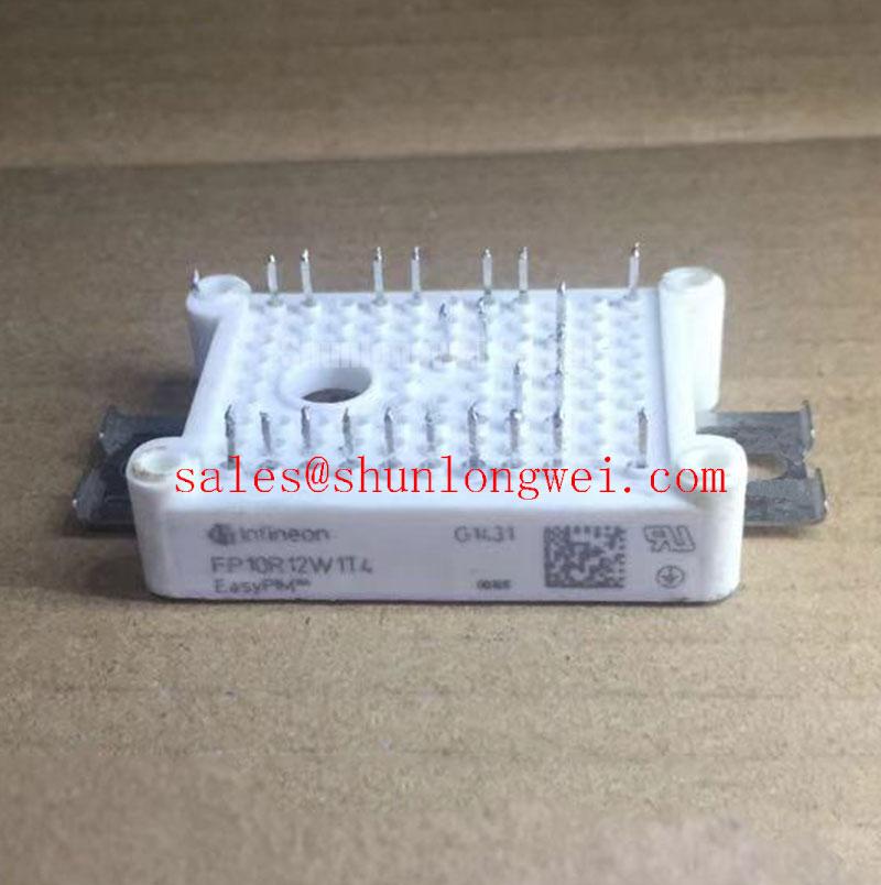
| Product Type | IGBT power module with inverter stage, input rectifier, and brake chopper |
| Inverter Stage Rating | 1200V VCES, 15A nominal collector current |
| Input Rectifier Rating | 1600V VRRM, 25A maximum forward current |
| Brake Chopper Rating | 1200V VCES, 15A continuous collector current |
| Thermal Rating | 0.85°C/W junction to case per IGBT |
Probe the desaturation sensing path and the actual gate to emitter waveform during a controlled fault response before returning a P840C4806 drive assembly to service. A desaturation event must be distinguished from a normal high-current switching transient by measuring the driver output, the collector voltage response, and the DC-link behavior on the same time reference. An apparent desaturation trip can originate in sensing-path noise, an incorrectly referenced measurement point, a driver supply disturbance, or a genuine load-side fault.
The P840C4806 integrates a 1200V, 15A inverter stage, while its input rectifier is rated at 1600V repetitive peak reverse voltage and 25A maximum forward current. Those ratings establish the module’s official electrical boundaries, but they do not define a driver’s trip threshold, blanking interval, or short-circuit timing. Type I and Type II desaturation terminology is commonly used at the gate-driver level; the actual response sequence depends on the protection controller and the complete inverter circuit.
A two-stage soft turn-off strategy is a Design Consideration where a fault response could otherwise force the collector current to fall too abruptly through a stray-inductive loop. The initial controlled discharge of the gate can reduce the tendency toward an excessive collector overshoot, followed by a secure off-state command once current has decayed. The oscilloscope record should show whether the collector voltage remains within the validated system margin against the DC-link voltage throughout that transition.
Inspect the sensing connection for a short, direct route to the monitored switching node and keep it separated from high-current commutation paths. A long shared return can inject voltage into the protection measurement and create a trip pattern that looks load-dependent. In a compact industrial inverter or a high-speed CNC spindle drive, compare the waveform under unloaded rotation, normal cutting load, and controlled deceleration. A change that follows switching edge speed rather than mechanical load points toward gate-loop or sensing-layout interaction.
🔧 Bench Diagnostic: De-energize the DC link and verify that stored energy has dissipated before moving probe grounds, gate-drive cables, or power connections.
Transient Dynamics & Electrical Design: High dv/dt Cross-Conduction Shoot-Through on P840C4806
Measure the off-state gate to emitter voltage of the complementary switch while its paired IGBT commutates, because an unexpected positive gate excursion is direct evidence of Miller-coupled turn-on risk. The test must use a measurement method that preserves the short gate loop; a long ground lead can add ringing that is absent at the module terminals. Inspect both the gate waveform and the DC-link current signature, since cross-conduction can appear as an abnormal current pulse even when the gate trace is difficult to interpret.
For the inverter stage of the P840C4806, high switching-node dv/dt can couple through device capacitances and shared inductance into an off-state gate circuit. A dedicated low-impedance active Miller clamp is a Design Consideration when the driver architecture supports it. A negative gate bias can also be assessed where the module’s qualified gate-drive conditions and the controller design permit it. Neither measure should be treated as a universal replacement for correct commutation-loop layout and verified dead-time behavior.
Gate-drive sourcing and sinking capability should be selected from the measured switching behavior, driver limits, and the required switching-loss versus overshoot balance. The external gate resistor is a tuning element rather than an arbitrary fixed value. Begin with the existing validated drive configuration where available, then evaluate turn-on and turn-off separately through double-pulse or equivalent switching tests. Excessively low damping can produce oscillation and false desaturation activity, while excessive damping can elevate switching loss and increase thermal stress.
Keep the gate return dedicated to the relevant emitter reference wherever the module connection scheme provides that possibility. Do not allow high-current power-return voltage to become the gate-drive reference. This separation is particularly important when service work changes cable dress, replaces a driver board, or reworks a busbar assembly. For related topology review in a separately assessed power stage, see FS15VE06VE3_B2; electrical interchangeability must be established from the complete circuit requirements rather than from a part number category.
P840C4806 Operational Boundaries: Evaluating Planar Symmetrical Busbar Geometry: Achievable Limits
Capture collector voltage at the module connection during turn-off and compare the measured peak with the DC-link voltage, because the difference helps reveal commutation-loop inductance and switching-rate interaction. In practical terms, peak collector voltage rises above the DC link by the product of loop inductance and current-change rate. This Engineering Calculation principle explains why a waveform that appears acceptable at reduced load can become problematic during a faster current transition or a fault-clearing event.
A planar, symmetrical busbar geometry is a Design Consideration for reducing the area enclosed by the outgoing and returning commutation paths. Place the DC-link capacitor connection close to the power module commutation loop, maintain paired conductor geometry, and avoid routing sensitive gate or desaturation conductors alongside high-current bus paths. The final inductance and allowable overshoot remain system-determined and should be verified at the intended DC-link voltage, switching frequency, load current, and thermal condition.
Snubber selection also requires waveform evidence rather than a generic capacitance prescription. A snubber can alter voltage overshoot and ringing, but it also changes stored energy, loss, and startup behavior. Observe the ringing frequency, the peak voltage, and the repeatability across operating points before judging whether the clamp network is effective. If the waveform varies substantially after a mechanical assembly change, check busbar contact surfaces, capacitor connections, and return-path symmetry before changing the gate resistor.
The P840C4806’s brake chopper is officially rated at 1200V VCES with 15A continuous collector current. In regenerative drive operation, validate brake-chopper switching independently from the inverter legs. A deceleration issue can involve the braking control signal, DC-link measurement, braking resistor circuit, or commutation layout; it should not be assigned to the module from a single symptom.
Where a repair assessment requires comparison with a different power-module platform, the BSM150GB120DLC page provides a separate reference point. Compare topology, electrical ratings, thermal interface, driver compatibility, and mechanical connection details as an engineering evaluation, not as a presumed replacement path.
P840C4806 Thermal-Electrical Optimization: Dynamic Power Loss Dissipation and Multi-RC Practical Tuning
Record heatsink temperature, switching waveform quality, and load current together during a repeated high-load cycle, because thermal diagnosis without electrical correlation can hide the source of loss. The official thermal value for the P840C4806 is 0.85°C/W junction-to-case resistance per IGBT. This value describes a junction-to-case path for each IGBT, not the full temperature rise through the thermal compound, mounting interface, heatsink, airflow path, or enclosure.
Peak junction-temperature margin cannot be calculated from junction-to-case resistance alone. It also requires switching and conduction losses, duty cycle, current waveform, case temperature, cooling conditions, and the applicable transient thermal model. A multi-RC model is useful when the official manufacturer thermal impedance information is available, because pulsed load behavior differs from a steady-state resistance approximation. In the absence of that model, use measured case temperature and validated electrical waveforms to guide investigation rather than presenting a calculated junction value as fact.
Thermal compound application, mounting flatness, and even clamping force affect the heat path. Treat installation practice as an Engineering Recommendation: use a clean mating surface, apply the thermal interface material consistently, and follow the specified mounting hardware procedure for the actual module and heatsink assembly. Uneven mechanical contact can produce localized temperature rise that may appear only after sustained loading, even when static electrical tests look normal.
Switching loss and temperature form a coupled loop. If a revised gate resistor reduces overshoot but slows a switching edge, reassess the thermal result under the real duty cycle. If cooling changes reduce case temperature but high-frequency ringing remains, correct the electrical layout problem rather than relying on the heatsink to compensate. For broader discussion of gate-drive interaction, thermal paths, and topology-level verification, consult IGBT Design & Integration.
Temperature-accelerated behavior is often discussed using the Arrhenius equation for semiconductor lifetime estimation, but no service-life prediction should be assigned to this module from that relationship alone. Use it as a Design Consideration when reviewing controlled reliability evidence, measured mission profiles, and the relevant manufacturer qualification data.