


Content last revised on October 4, 2026
PD10016 Circuit Protection and Reliability: Calibrating AC Input Transient Overvoltage Clamping
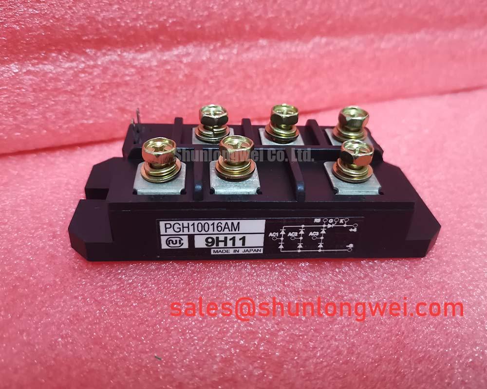
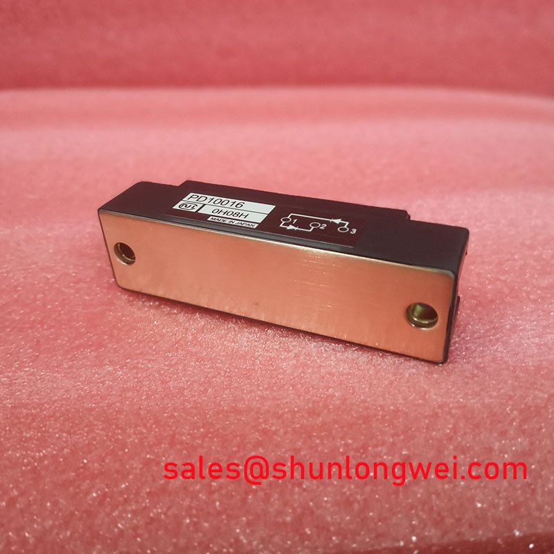
For a grid tied Static Var Compensator or thyristor switched capacitor assembly, the PD10016 should be evaluated as one part of the AC power path rather than as a stand alone protection device. An engineering design consideration is to place the input protection network, semiconductor fusing, and commutation suppression elements according to the measured system fault level and switching waveform. Metal oxide varistors may be assessed for the expected temporary overvoltage, surge energy, and repetitive duty, while an RC snubber network may be evaluated around the thyristor path when switching transients are observed.
The official ratings of 1600.0 V and 100.0 A do not by themselves define the permissible MOV selection, fuse clearing time, or snubber values. Designers should verify the actual repetitive peak voltage, surge waveform, line impedance, and thermal operating point in the completed assembly. IEC 61000-4-5 may be used as a design reference for surge testing, but compliance of the finished SVC equipment cannot be assigned to the module alone. Power semiconductor application references, including the Shindengen power semiconductor module resources, can support the wider protection review.
During maintenance, inspect the AC terminals for discoloration, looseness, and evidence of localized heating. Confirm that the cable arrangement matches the original power path and keep high current conductors physically separated from sensitive gate or monitoring wiring. The manufacturer installation document should control the permitted terminal hardware, contact surface condition, and mounting torque because no torque value is established by the supplied PD10016 specifications.
PD10016 Circuit Protection and Reliability: Calibrating Short Circuit Withstand Limits
Short circuit coordination requires comparison between the selected semiconductor fuse clearing characteristic and the module’s documented surge withstand data. The PD10016 listing confirms voltage, current, and package class, but it does not provide a fuse I²t coordination table in the supplied parameter set. An engineering recommendation is therefore to obtain the manufacturer’s relevant transient, surge, and thermal curves before approving a fuse for a dead short condition.
In the service bay, isolate the DC link and verify that stored energy has decayed using the equipment’s approved discharge procedure. Inspect the fuse body, busbar joints, and module terminals together, since a healthy replacement module cannot correct a loose connection or an incorrectly coordinated protective device. Where a short circuit has occurred, compare phase resistance and gate circuit continuity with a known good assembly, then use controlled low energy testing before returning the SVC to full voltage.
For a higher current branch or a different physical arrangement, engineers may also assess the related PD25016A as a separate replacement candidate. It should not be treated as an automatic substitute: voltage class, current duty, circuit topology, terminal layout, thermal interface, and protection coordination must all match the original design.
Assembly Integrity and Layout Architecture: Implementing ITSM Safety Derating across Repetitive Switching
Repeated capacitor switching can expose the module to short duration current pulses that differ substantially from its continuous current rating. The PD10016 official current specification is 100.0 A, but no ITSM, pulse duration, transient thermal impedance, or junction temperature curve is included in the supplied data. Those values must not be inferred from the continuous rating. Before approving repetitive operation, the system engineer should verify the manufacturer’s sinusoidal half cycle surge data and compare it with measured pulse current, repetition rate, heat sink condition, and junction temperature recovery.
Layout work should minimize the shared impedance of the power and control return paths. If the particular module version provides auxiliary or Kelvin style control terminals, those terminals should be routed according to the manufacturer’s terminal drawing and kept separate from the high di/dt power loop. Do not assume an auxiliary terminal function or pin arrangement without the original mechanical and electrical documentation. Gate wiring should be checked for common mode ground bounce during switching tests, and any negative off bias should be treated as a system design choice requiring confirmation of the module’s gate limits.
Dust accumulation on the heat sink, aged thermal interface material, blocked airflow, and condensation can shift the operating temperature even when electrical loading appears normal. ⚠️ Maintenance Note: Monitor contact temperature during scheduled service and verify that the heat sink air path remains clean and dry before retightening or replacing the module.
Transient Dynamics and Electrical Design: Minimizing Commutation Turn Off Voltage Spikes on PD10016
Commutation testing should capture the voltage across the module and the current in the shortest practical measurement loop, using probes and bandwidth suitable for the switching edge. Reverse recovery peak current, recovery time, soft recovery behavior, and commutation overshoot are not supplied as official PD10016 parameters here, so they must be verified from the manufacturer’s detailed datasheet or measured on the actual circuit. The 1600.0 V rating is an electrical boundary, not permission to expose the device to uncontrolled repetitive overshoot.
Designers should minimize parasitic loop inductance and place the suppression network with a short connection to the power terminals, then verify peak voltage against the system DC link and AC switching conditions. If EMI is detected, distinguish conducted disturbance from radiated coupling by checking the gate return, enclosure bonding, probe ground method, and cable routing. The module itself cannot be described as independently passing a complete EMC certification for the finished equipment.
For upstream topology review, the PD104VT2T1 may be evaluated as a related rectification or complementary power stage, subject to the circuit schematic and electrical ratings. For gate control research, the Evolution of Negative Off Bias Gate Drive Circuits provides relevant background, while the final gate voltage, isolation method, and transient testing remain determined by the complete SVC design.