



Content last revised on October 6, 2026
Assembly Integrity and Layout Architecture for the GD400SGX170C2S
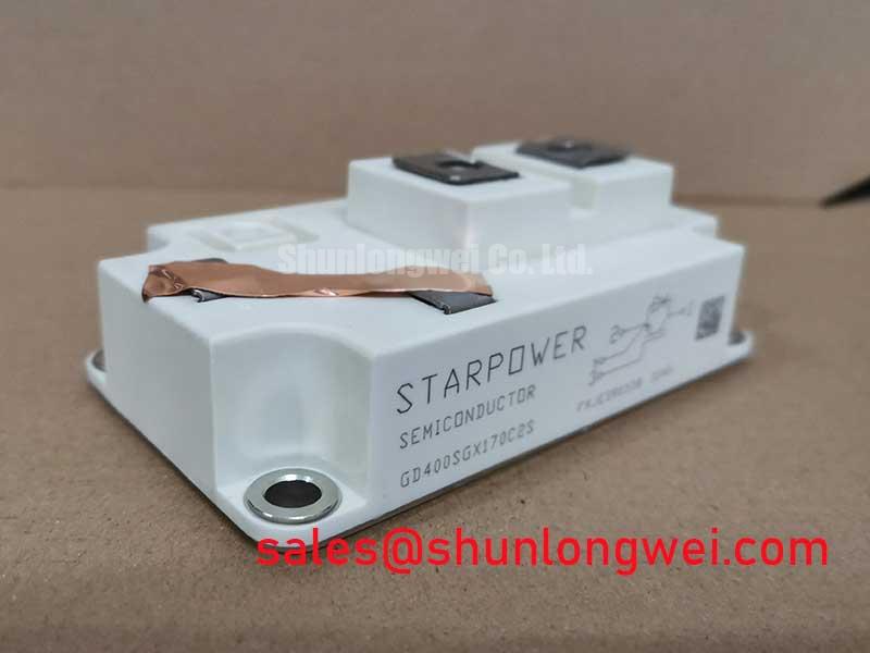
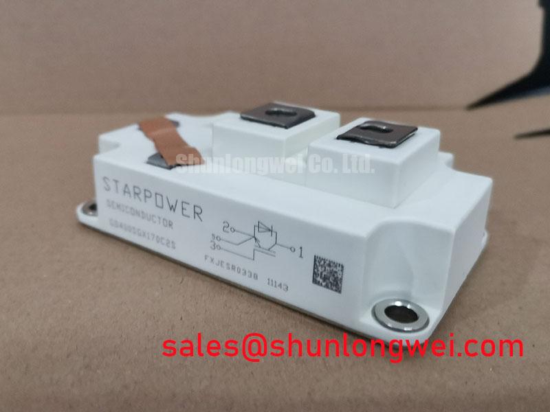
Use ESD protection before testing, then compare the module’s marked terminals with the approved circuit documentation and perform a cold-state resistance check between the power terminals before applying any gate signal. The GD400SGX170C2S is a StarPower IGBT Module with a rated voltage of 1700 V and a rated current of 400 A. Its listed package format is Module.
| Parameter | Official Product Information |
|---|---|
| Manufacturer | StarPower |
| Model | GD400SGX170C2S |
| Rated voltage | 1700 V |
| Rated current | 400 A |
| Package | Module |
These ratings identify the component category and electrical scale, but they do not by themselves establish a complete operating point for a solar inverter, motor drive, braking chopper, or other high-power converter. The system engineer should verify switching frequency, gate-drive conditions, cooling performance, overload duration, short-circuit coordination, and the applicable electrical clearances against the original equipment documentation.
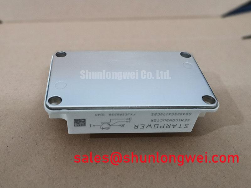
For incoming inspection, first record the package marking and inspect the external case, terminals, mounting surface, and insulation areas under controlled lighting. Look for bent terminals, contamination, cracks, loose hardware, or marks that could interfere with the intended mounting surface. The terminal polarity and functional identity should be checked against the manufacturer’s approved drawing rather than inferred from a similar module.
A multimeter diode test can be useful when the approved terminal map identifies an antiparallel diode path. Measure in both polarities with the module isolated from the circuit, note the cold-state readings, and compare them with a known-good reference of the same configuration. This is a screening procedure, not a substitute for a controlled insulation, gate, or dynamic switching test. A low-resistance reading can also be influenced by external capacitors, snubbers, current-sense circuits, or parallel semiconductor paths if the module remains connected to the converter.
When evaluating the GD400SGX170C2S for a high-power photovoltaic inverter, thermal analysis should begin with the actual load profile rather than the nominal current alone. A junction-to-case transient thermal model can represent the module’s heating response during switching pulses, overload events, and regenerative or braking-related energy transfer. The engineer may use a multi-RC network to estimate junction temperature from the measured power waveform, but the thermal impedance values and pulse interpretation must come from the applicable device documentation or validated measurement data.
The useful engineering workflow is to capture collector-emitter voltage, current, switching duration, and case temperature during representative tests. The resulting loss waveform can then be applied to the selected transient thermal model. Peak junction-temperature margin is determined by the complete combination of semiconductor loss, case temperature, heatsink performance, interface condition, airflow or liquid cooling, and overload repetition. It should not be inferred from the 400 A rating in isolation.
Layout planning should keep high-current commutation paths short and physically compact while maintaining the isolation distances required by the system voltage and applicable safety standard. The DC-link loop, module terminals, snubber network, and busbar geometry should be reviewed together because stray inductance can produce turn-off voltage overshoot. Designers should verify peak voltage during switching tests against the actual DC-link condition instead of assigning a universal clearance or inductance value to every installation.
Thermal-Electrical Optimization and Gate-Drive Loop Geometry
The gate-drive connection deserves a separate review from the main power path. Where the module provides an auxiliary emitter or control return, the driver return should follow the intended control reference and should not share a long, high-current emitter route. Separating the gate-drive return from the main power-current path is a design consideration for reducing emitter mutual coupling and unwanted voltage feedback during rapid current change.
During bench evaluation, apply the approved gate signal with the power stage disabled first. Check the gate-to-emitter waveform at the module terminals, not only at the driver output, because cable inductance, connector resistance, and common return impedance can change the voltage seen by the semiconductor. Designers should verify turn-on and turn-off timing, dead-time behavior, Miller-related disturbances, and any negative or positive excursions against the driver and module documentation.
Dead-time selection is system-determined. It must prevent cross-conduction under the actual propagation delay, temperature, load current, and driver conditions while avoiding unnecessary diode conduction and switching loss. A gate resistor or damping network may be tuned from a conservative starting point, but the final value should be established with an oscilloscope and double-pulse or equivalent switching tests. The module’s official documentation should be used for any gate-voltage limit, gate-charge value, or short-circuit operating boundary.
For high-power inverter service, fuse coordination should be checked as a complete fault-clearing study. The semiconductor fuse I²t characteristic, prospective fault current, DC-link energy, wiring inductance, and the module’s documented short-circuit or surge capability all affect whether a protective device can interrupt the fault within the required time. A fuse selected only from the normal current rating may not provide suitable sub-cycle protection. The resulting coordination should be verified through the manufacturer’s fuse data and the converter protection test plan.
In a regenerative braking chopper or a high-power braking resistor branch, the switching device must be evaluated against the actual DC-link overvoltage profile and resistor energy duty. The braking resistor, chopper control, fuse, bus capacitor, and thermal system operate as one protection network. Engineers should verify the resistor’s pulse-energy capability and the chopper’s switching stress during worst-case deceleration or grid disturbance conditions.
For current feedback and protection circuits, the signal chain should be reviewed for bandwidth, common-mode range, layout coupling, and fault response. Reference material on current-sense amplifier architectures is available from ADI current-sense amplifier resources. This industry reference does not define the GD400SGX170C2S application circuit; it is useful when assessing the measurement path around the power module.
Transient Dynamics and Reinforced Insulation Barrier Integrity
Isolation requirements should be confirmed from the complete inverter architecture rather than assumed from the presence of an IGBT module. The module, gate driver, isolated power supply, PCB slots, busbar supports, heatsink, and enclosure may all contribute to the insulation system. If a design requires a reinforced isolation barrier, the responsible engineer must verify the required withstand voltage, creepage, clearance, pollution environment, and certification basis from the relevant component and system documentation.
Common-mode transient immunity is also a property of the complete gate-drive signal chain. A digital isolator or optocoupler may have a specified CMTI value, but the practical result depends on driver layout, isolated supply behavior, grounding, parasitic capacitance, and the switching waveform at the module terminals. Do not treat an assumed CMTI threshold as an official specification of the GD400SGX170C2S. Instead, measure the gate signal during high-voltage switching and check for false pulses, abnormal duty-cycle changes, or driver supply disturbance.
A controlled diagnostic sequence begins with a de-energized visual inspection, followed by continuity checks on the gate-drive board, isolated supply verification, and comparison with a known-good signal path. Oscilloscope probes must be selected and connected so that the measurement method does not create an unintended path across the isolation barrier. If the observed waveform differs between the driver output and the module terminals, investigate the connector, return path, probe reference, and parasitic coupling before attributing the condition to the IGBT itself.
The Wide Bandgap Revolution engineering guide provides broader context on fast-switching power semiconductor layout and transient behavior. Its discussion should be treated as general design guidance, not as a replacement for the StarPower documentation applicable to this silicon IGBT module.
💡 Bench Tip: Keep the module isolated from the powered converter, use ESD controls, and record cold-state readings before comparing diode-path or gate-to-emitter behavior with a reference device.
Baseplate Contact, TIM Control, and Sequential Fastening
The thermal interface is part of the electrical and thermal installation, even though it is not an official rating of the module. The heatsink surface should be clean, flat within the equipment manufacturer’s specified tolerance, and free from burrs or particles that could create local pressure points. Apply the selected thermal interface material consistently and avoid excessive compound that could increase bond-line thickness or migrate toward insulation surfaces.
Where a baseplate shows measurable curvature, the assembly engineer should evaluate contact pressure distribution instead of attempting to correct the condition by uneven screw loading. A fixture, compliant interface, or approved mounting method may be appropriate, but the permitted approach depends on the module construction and heatsink design. Double-sided cooling arrangements require the same discipline on both thermal paths: inspect parallelism, verify contact imprint after a controlled trial assembly, and confirm that the final pressure does not distort the package.
Fasteners should be tightened in the sequence and to the torque specified by the applicable StarPower mechanical drawing or equipment assembly procedure. If no model-specific torque is available in the working documentation, the value must be selected by the mechanical designer from the fastener size, thread material, washer arrangement, clamping target, and module mounting requirements. A generic torque value should not be presented as an official parameter of the GD400SGX170C2S.
After assembly, measure case temperature at comparable load points and inspect the thermal response during controlled power testing. A local hot spot, unexpected temperature imbalance, or unstable case reading may indicate interface nonuniformity, heatsink distortion, sensor placement effects, or an electrical imbalance. Confirm the mechanical installation and current sharing before replacing the module.
For substitution assessment, the BSM400GA120DN2S_E3256 may be reviewed as a separate candidate only after its voltage, current, terminal arrangement, gate requirements, mechanical dimensions, thermal interface, and protection limits have been matched to the original design. It should not be treated as an automatic replacement. For a separate converter stage, engineers may also examine the FP10R12KE3 as a related component for topology-level evaluation, subject to that stage’s requirements and the original equipment documentation.