

Content last revised on September 12, 2026
PHMB300B12 Circuit Protection & Reliability: Calibrating Managing High C Rate Battery Cycling Swing
Measure the DC link voltage ripple, module case temperature trend, and gate drive timing during repeated battery charge and discharge transitions before replacing the PHMB300B12 in a commercial string inverter or micro grid energy storage cabinet. A 1200 V, 300 A IGBT power module can operate inside a bidirectional conversion stage, but the surrounding control system determines how quickly current reverses, how the DC battery rack responds, and whether switching transitions remain inside the intended electrical boundary.
During high C rate battery cycling, a converter can move power from the battery rack to the inverter DC link during discharge, then reverse the direction while charging. This bidirectional operating behavior causes recurring current reversal, changing diode conduction intervals, and repetitive temperature movement across the power stage. The module itself must be evaluated as part of the complete switching path: DC capacitors, laminated busbars, gate driver supply, current sensors, cooling plate, battery contactors, and control firmware all influence the electrical stress seen at the terminals.
Field troubleshooting should start with a controlled shutdown, discharge verification at the DC link, and inspection of the main terminal interfaces for discoloration, loosened hardware, insulation damage, or uneven pressure marks. Cold resistance checks can help identify an obvious short circuit condition between main terminals, but they do not verify dynamic switching health. A module can show no direct short on a handheld meter while the active gate circuit, freewheeling path, or driver timing still requires investigation under controlled waveform measurement.
Design Consideration: keep the high current commutation path physically compact and use a low inductance DC link arrangement where the system layout permits it. This helps limit turn off overshoot created when current changes rapidly through unavoidable stray inductance. The system engineering team should verify peak collector emitter voltage, current ringing, and gate behavior against the DC link voltage during double pulse or controlled load switching tests.
Repeated battery cycling also makes thermal contact quality important. A changing power profile can reveal cooling path weaknesses that remain hidden during a short bench run. Monitor the relationship between cooling plate temperature, measured current, ambient condition, and protective fault timing. A gradual increase in thermal response may indicate degraded thermal interface contact, restricted coolant flow, fan degradation, heat sink contamination, or a control change that has shifted the switching burden.
For system level study of switching device selection, protective coordination, and reliability validation practices, engineers can refer to the Power Electronics Masterclass. It is useful when determining whether a recurring field fault originates in the module, driver logic, DC link layout, cooling system, or battery management command sequence.
- Record battery current direction and DC link voltage at the instant of protection trips.
- Compare gate command timing across parallel inverter legs where the original controller provides comparable test points.
- Inspect DC bus capacitor connections and busbar joints for signs of heat concentration.
- Verify that current sensors and battery management commands are not producing an unintended rapid reversal request.
- Review cooling system operation under sustained charge and discharge duty rather than idle operation alone.
Transient Dynamics & Electrical Design: High dv/dt Cross Conduction Shoot Through on PHMB300B12
Probe the gate emitter waveform of both switches in the affected inverter leg while observing the collector emitter transition when shoot through, overcurrent shutdown, or irregular current spikes occur. In a PHMB300B12 installation, rapid voltage movement at one device can couple through gate capacitances and shared emitter inductance into the complementary device gate loop. If the inactive device gate rises enough during the transition, temporary cross conduction can occur and sharply increase DC link current.
Design Consideration: use a dedicated low impedance gate return path and evaluate active Miller clamp behavior where the driver architecture supports it. A negative gate bias can also be used as a system dependent measure against unintended turn on, but the selected voltage must be verified against the gate driver, insulation coordination, switching waveform, and the applicable device documentation. The requested negative bias range is commonly discussed in the industry, yet no fixed setting should be assigned to this specific module without full driver and waveform validation.
Check whether the driver output, gate resistor network, clamp path, and emitter reference are physically close to the intended gate loop. Long shared return paths can create a misleading gate voltage reading and can also inject switching noise into the driver reference. Oscilloscope probing must use a measurement method suitable for fast power switching; an unsuitable probe ground arrangement can introduce noise that looks like a real gate disturbance.
The freewheeling diode commutation interval deserves equal attention. Reverse recovery behavior can interact with busbar inductance and switching speed, producing collector voltage ringing that complicates both EMC performance and gate stability. A snubber network can be evaluated as a Design Consideration when waveform capture shows excessive ringing, but its component values, placement, loss budget, and thermal impact must be established by the converter design team through measured testing. Do not treat a snubber as a universal correction for an incorrect gate loop or weak DC link layout.
The physical principles of IGBT switching, gate control, and intelligent module integration are also discussed by ROHM Field Stop Trench IGBTs and Intelligent Modules. That technical context is relevant when assessing why drive loop inductance, commutation current, and diode recovery can affect switching behavior even when the measured DC bus voltage appears stable.
For a topology containing a separate rectifier or auxiliary power stage, the interaction of upstream commutation current and inverter switching should be checked rather than assumed. The CM300HA-24E is a related power semiconductor reference that may be evaluated within a broader converter architecture, subject to verification of circuit topology, terminal arrangement, thermal interface, and drive requirements.
When desaturation protection is used, confirm that the sensed collector emitter voltage is interpreted only after the normal switching blanking interval established by the driver designer. A rapid hard shutdown during a genuine short circuit can create a high inductive voltage event. Soft turn off behavior is therefore a system protection function that must be checked with the actual busbar, gate driver, current path, and fault energy conditions.
PHMB300B12 Operational Boundaries: Evaluating Baseplate Thermal Grease Layer Control Limits
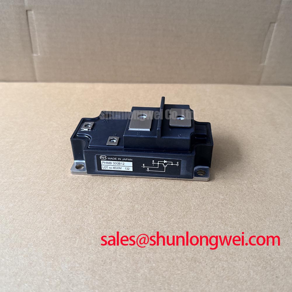
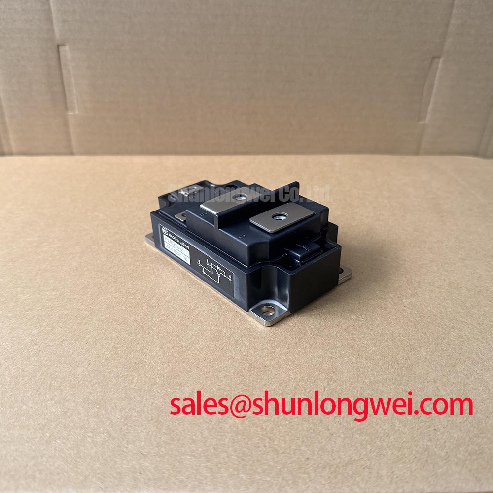
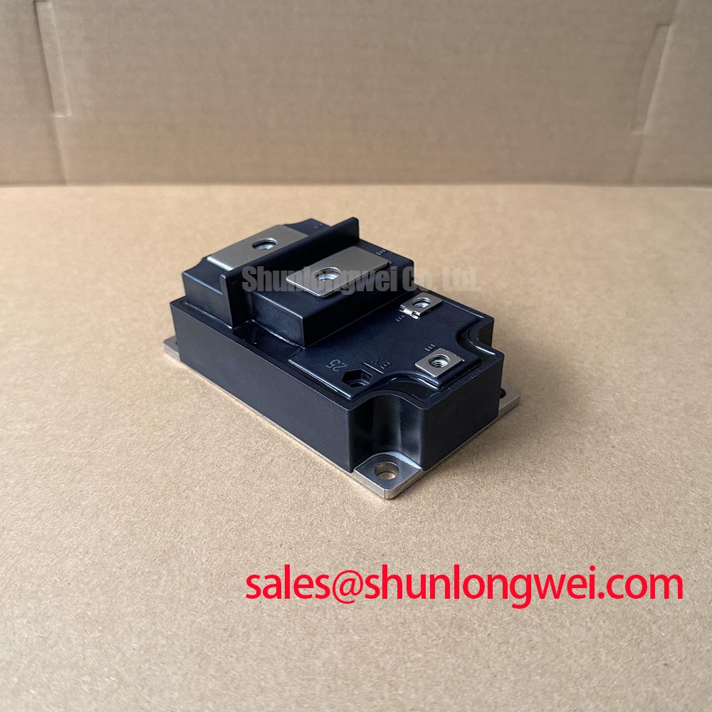
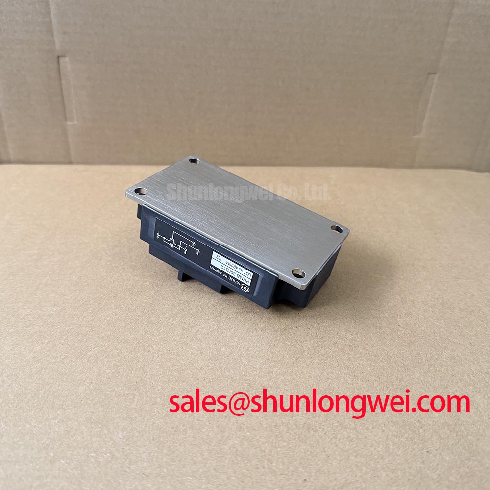
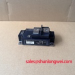
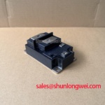
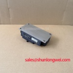
Inspect the thermal grease imprint across the module mounting footprint immediately after removing a suspect unit, because dry zones, thick ridges, trapped debris, or uneven compression can explain a localized temperature rise. The PHMB300B12 is supplied as a Power Module, and its case to heat sink interface is a critical part of the installed thermal path even though cooling system dimensions and mounting hardware are determined by the equipment builder.
Engineering Recommendation: apply thermal interface material as a thin, uniform layer intended to fill microscopic surface irregularities rather than create a thick insulating pad. A general industry assembly reference often places controlled grease layers within approximately 50 to 100 μm, but the actual target must follow the thermal material supplier guidance, module mechanical drawing, cooling plate flatness, and equipment assembly procedure. Excess material can increase thermal resistance; insufficient coverage can leave air voids and reduce heat transfer.
Check the cooling plate surface for scratches, corrosion, burrs, embedded particles, and distortion around previous mounting points. Baseplate curvature and heat sink flatness can change the pressure distribution after fastening. If a module repeatedly shows one side running hotter than the other under similar current, inspect mounting sequence and heat sink contact before assigning the issue to semiconductor wear.
Use a sequential tightening pattern that distributes pressure gradually across the module baseplate. The final torque must follow the original hardware specification for the screw type and mounting arrangement. ⚠️ Field Alert: Tighten mounting hardware progressively in sequence and keep thermal grease coverage uniform, because uneven clamping can distort the thermal interface and create avoidable hot spots.
After reassembly, run a controlled load test while recording temperature response at repeatable operating points. Compare results with the same cooling flow, ambient condition, and switching pattern used before service. A thermal result that changes after reinstallation may indicate interface quality, cooling plate condition, sensor placement, or altered control duty rather than a single component fault.
For commercial string inverter and micro grid energy storage systems, cooling behavior must be reviewed across both battery charging and discharge operation. The direction of energy flow changes current paths and switching intervals, while the cooling system remains responsible for removing total converter loss. Engineers should verify that fan control, pump control, airflow channels, coolant flow, and cabinet filters remain consistent during the load profile that previously produced the alarm.
PHMB300B12 Circuit Protection & Reliability: Calibrating Multi Module Parallel Current Sharing
Capture current and gate waveforms from each parallel module position during a controlled load ramp when one PHMB300B12 location runs hotter or reaches protection earlier than the others. Parallel IGBT positions do not automatically share current equally simply because each module has the same nominal 1200 V and 300 A rating. Static current distribution, dynamic switching distribution, busbar geometry, gate loop symmetry, cooling contact, and controller timing all need examination.
At steady state, IGBT modules can exhibit a positive temperature coefficient in the relevant operating region, which can support static current sharing under appropriate conditions. This is a Design Consideration rather than a guarantee of equal sharing. Dynamic imbalance can still occur when one position has a shorter gate loop, lower gate resistance, different emitter reference path, lower busbar inductance, or a faster local driver response.
Start by comparing the physical path from each driver output to its gate and return reference. Parallel positions should use symmetrical gate wiring principles so that switching command propagation and induced noise are comparable. Then inspect the main current paths from the DC link capacitor to each module and from each module to the output connection. A difference in conductor length, joint condition, or laminated busbar placement can shift commutation stress toward one device.
Where the converter uses individual desaturation sensing or current feedback per module position, compare the protection threshold behavior and blanking arrangement under the same controlled test. An early trip in one position may reflect a real current imbalance, sensing path noise, reference movement, or a driver circuit issue. Confirm findings with synchronized waveform captures instead of relying on a single temperature sensor or a single current reading.
Thermal symmetry matters as much as electrical symmetry. Check that each parallel module has comparable cooling plate contact, grease coverage, clamping sequence, and airflow or liquid cooling exposure. A cooler module can take more current in some conditions, while a hotter location can reach protective limits earlier. The correction should address the observed physical imbalance rather than assume that electrical matching alone will solve it.
When evaluating an alternative module family during equipment repair planning, compare topology, terminal layout, driver compatibility, protection behavior, package dimensions, cooling interface, and validated switching performance. The CM300DY-24A comparison resource provides a neutral reference for examining cross model considerations without treating any alternative as an automatic replacement for the PHMB300B12.
For a parallel inverter bridge, the practical acceptance test is a repeatable comparison of current sharing, gate waveform shape, collector emitter transition, thermal response, and protection timing under the same operating condition. The final decision on continued service, driver adjustment, busbar revision, or module replacement belongs to the system engineer after those measurements are correlated with the original converter requirements.