
Content last revised on September 16, 2026
Transient Dynamics & Electrical Design: High Frequency Common Mode Bearing Current on PM100CVA060
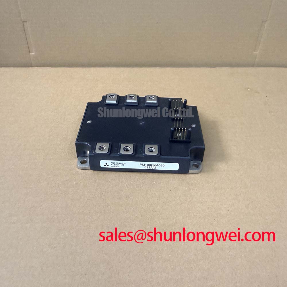
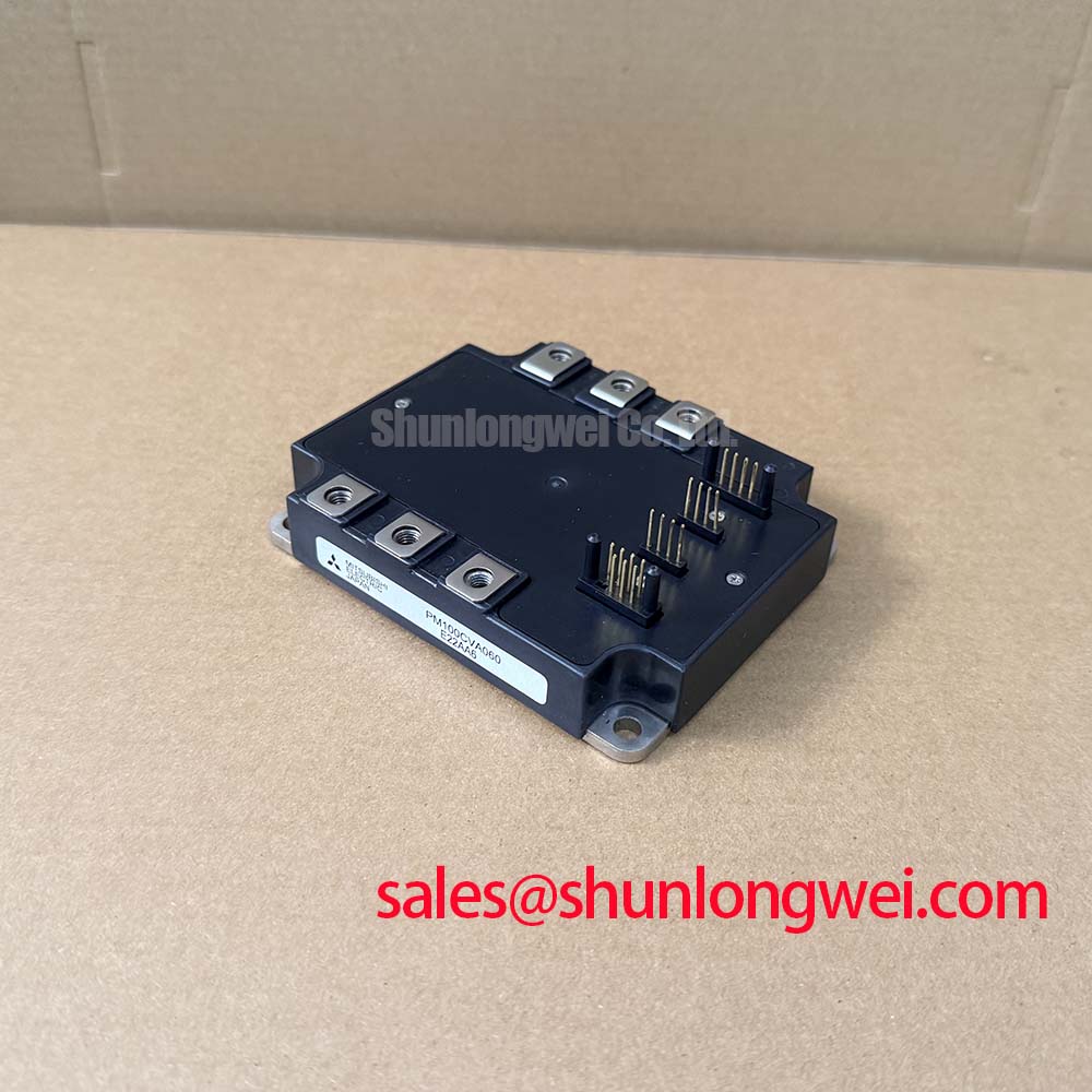
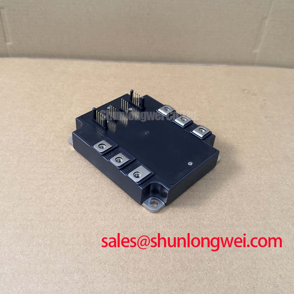
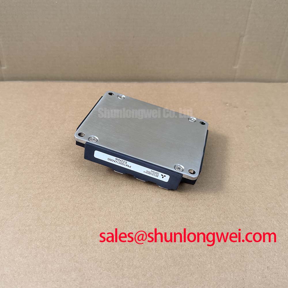
The PM100CVA060 is a Mitsubishi Electric IGBT module specified at VCES = 600V and IC = 100A at case temperature of 25°C. Its 200A peak collector current rating is an Official Datasheet Specification for transient current capability, but it must not be treated as an unrestricted repetitive surge allowance. In industrial inverter welders and medium frequency induction heating supplies, the real electrical boundary is set by the DC link voltage, switching waveform, commutation current, thermal condition, and the energy stored in external inductance.
A long output cable between an inverter and a remote load can behave as a transmission line rather than a simple conductor. When a fast switching edge reaches an impedance discontinuity, the reflected voltage can add to the incident waveform. Under unfavorable cable and load conditions, reflected terminal voltage can approach twice the DC bus voltage. This is a Design Consideration, not an official PM100CVA060 voltage withstand statement. The system engineer should capture voltage directly at the module and load terminals with suitable differential measurement equipment, then verify peak margins against the 600V collector emitter rating.
Where the equipment topology drives a motor, common mode voltage can also circulate through cable capacitance, machine frame paths, and bearing structures. Bearing current is not caused by the PM100CVA060 alone. It depends on motor construction, cable routing, inverter output waveform, grounding arrangement, and parasitic capacitances. In a service investigation, inspect cable shields, protective earth continuity, output reactor connections, and filter capacitor condition before attributing bearing damage or unexplained ground current to the power module.
Engineering Recommendation: keep the high current commutation loop physically compact, maintain controlled spacing between positive and negative DC link conductors, and place DC link capacitors so that switching current does not travel through a long busbar path. The objective is to reduce inductive overshoot during turn off. Final busbar geometry, output choke selection, and dv/dt filter performance must be confirmed in the completed converter under its actual DC bus and load conditions.
For inverter welder repairs, an output choke with changed inductance, a loose laminated busbar, or an incorrectly routed welding cable can alter switching stress even when the replacement module is electrically sound. For induction heating equipment, verify the resonant tank, work coil connections, and current feedback path because detuned load conditions can raise semiconductor stress without a visible fault on the controller board.
| Official PM100CVA060 Specification | Value | Integration Relevance |
|---|---|---|
| Collector emitter voltage, VCES | 600V | Verify against measured DC link and switching overshoot |
| Collector current at TC = 25°C, IC | 100A | Continuous current reference under stated case temperature condition |
| Peak collector current, ICP | 200A | Transient capability reference, not a repetitive operating prescription |
| Collector dissipation at TC = 25°C, PC | 338W per switch | Thermal evaluation starting point |
| IGBT VCE(sat) | 2.35V typical, 2.80V maximum at 100A | Relevant to conduction loss and desaturation protection assessment |
| Isolation voltage, Viso | 2500Vrms for 1 minute | Baseplate isolation specification |
| IGBT thermal resistance, Rth(j c) | 0.37°C/W maximum per switch | Junction to case thermal path |
| Diode thermal resistance, Rth(j c) | 0.70°C/W maximum per diode | Freewheel diode thermal path |
PM100CVA060 Circuit Protection & Reliability: Calibrating Isolated DC DC Power Supply Sizing for High Current Switching
The PM100CVA060 baseplate isolation rating is 2500Vrms for one minute, an Official Datasheet Specification. This value identifies the module baseplate isolation test condition and should not be confused with the required insulation coordination of the complete inverter. Isolated gate drive supplies, current sensors, controller communications, enclosure earth paths, and external wiring must be assessed separately by the system designer.
For a repair bench, confirm that isolated auxiliary supplies reach their intended regulated levels before reconnecting the DC bus. A supply that rises slowly, collapses under gate drive demand, or carries excessive switching noise may create irregular turn on behavior that resembles a failed IGBT. The available power for isolated DC DC converters must cover gate driver consumption, isolation requirements, startup behavior, and fault response requirements of the actual control board.
Design Consideration: many high energy converter control systems use reinforced galvanic isolation and high common mode transient immunity to prevent switching edges from creating false gate commands. Values such as isolation withstand above 5kV and common mode transient immunity above 100kV per microsecond are system level targets sometimes evaluated by designers, not PM100CVA060 factory ratings stated here. The original driver documentation and applicable insulation standards must determine the required values.
Desaturation monitoring is commonly used to detect an abnormal rise in collector emitter voltage while a switch is commanded on. The 2.35V typical and 2.80V maximum VCE(sat) values at 100A are Official Datasheet Specifications, yet a protection threshold cannot be selected from those figures alone. It is affected by temperature, load current, diode recovery, blanking interval, measurement network behavior, and switching noise. A short circuit response interval below 3 microseconds can be a system protection objective in some designs, but it is not a specified PM100CVA060 protection delay.
Where a controller uses a two stage soft turn off routine, its purpose is to reduce the risk of excessive inductive voltage during fault interruption. The correct turn off profile depends on the DC link, stray inductance, busbar layout, and protection circuit. Verify the waveform with the intended probe arrangement instead of changing gate resistor values by assumption.
For a broader engineering reference on inverter switching, reliability boundaries, and protection verification, consult the Power Electronics Masterclass. Mitsubishi Electric also provides a useful external reference on DIPIPM™ bootstrap circuit design, particularly when reviewing driver supply behavior and high side control arrangements.
Field Diagnostics & Commissioning: Symmetrical Busbar Geometry for High Current PM100CVA060 Topologies
Before commissioning a repaired inverter, compare each DC bus connection path from the capacitor bank to the PM100CVA060 and back to the return conductor. Unequal conductor length, different fastener stack height, an offset busbar, or a missing insulating spacer can create unequal parasitic inductance. That imbalance can change dynamic current distribution during switching, even when static resistance readings appear similar.
The PM100CVA060 has a maximum IGBT junction to case thermal resistance of 0.37°C/W per switch and a maximum freewheel diode junction to case thermal resistance of 0.70°C/W per diode. These Official Datasheet Specifications support thermal path assessment, but they do not establish heatsink performance, grease thickness, airflow, water flow, or cabinet ambient temperature. A module can show normal cold resistance checks while still overheating due to poor contact between baseplate and heatsink.
When checking a removed module, use the meter only as a screening tool. Compare corresponding power paths and control terminal behavior against a known good assembly or the original circuit documentation. An unexpected low impedance, open path, or inconsistent result may indicate damage, contamination, meter lead error, or interaction with connected circuitry. Isolate the module from surrounding gate drive and snubber networks where practical before drawing conclusions.
Static current sharing in parallel power paths cannot be guaranteed from a single VCE(sat) figure. Semiconductor voltage characteristics vary with current and junction temperature, while dynamic sharing is heavily influenced by gate drive timing and busbar geometry. Where multiple power modules are used in parallel, designers should verify matched electrical paths, thermal coupling, gate command timing, and measured current distribution under controlled load conditions.
⚠️ Field Alert: Tighten power terminals and heatsink hardware according to the equipment manufacturer’s fastener specification, using a clean flat mounting surface and an even thin thermal interface layer before energizing the DC bus.
For an inverter welder, inspect rectifier connections and DC link capacitor terminals after any high current fault because a loose upstream joint can produce heat and voltage ripple that later appears as an IGBT problem. In phase controlled front ends, firing angle errors and supply distortion can also alter the DC bus waveform. Harmonic mitigation must be evaluated at system level through measured line current and applicable installation requirements, not assigned to the PM100CVA060 module.
If a replacement assessment requires comparison with another Mitsubishi power module family, the CM100DY-12E should be reviewed only against the original schematic, terminal arrangement, voltage class, current conditions, thermal interface, driver compatibility, and protection implementation. Similar current numbers alone do not establish interchangeability.
Field Diagnostics & Commissioning: Optimizing Gate Drive Loop Geometry to Prevent Oscillation in PM100CVA060 Topologies
Gate loop problems often appear first as unstable collector emitter waveforms, irregular current traces, repeated protection events, or unexplained heating after a board repair. Start by checking gate driver connector seating, damaged traces, contaminated control headers, return path continuity, and the placement of any gate damping parts specified by the original equipment design. Do not alter the gate network until the original connections and fault signals have been verified.
Engineering Recommendation: separate low level gate drive return paths from the main high current emitter or power return conductors wherever the actual module terminal arrangement and original driver layout support this practice. The aim is to reduce mutual inductive coupling that can feed switching current noise into the gate control reference. The PM100CVA060 terminal documentation should be checked before assuming that a separate auxiliary emitter or control return terminal is available.
During oscilloscope work, probe placement matters as much as the waveform itself. Long probe ground leads can capture radiated noise and make ringing appear worse than it is. Use measurement techniques appropriate for high voltage switching nodes, confirm that the test instrument has the required isolation rating, and compare the waveform at consistent locations before judging a change in gate loop routing.
The 338W collector dissipation per switch rating at case temperature of 25°C is an Official Datasheet Specification, not a usable cabinet dissipation allowance. Conduction loss depends in part on VCE(sat), while switching loss depends on operating conditions that are not specified in the provided parameter set. Thermal validation should therefore include measured case temperature, cooling system condition, current waveform, switching behavior, and load duty cycle.
For systems exposed to unusual altitude, radiation environment, severe mains disturbance, or extended unattended operation, no PM100CVA060 failure rate, cosmic ray tolerance, single event burnout margin, or operating life figure should be inferred from the specifications above. Those matters require equipment level validation and authoritative environmental or reliability documentation. Mitsubishi Electric’s high voltage power semiconductor information provides additional manufacturer context for evaluating power device families alongside the original system requirements.