




Content last revised on September 30, 2026
PM50B6LA060 Operational Boundaries: Evaluating Desaturation Detection Limits
Measure the gate, emitter, and power terminals with the module fully isolated from the DC link, then compare the cold-state readings with a known-good reference before applying any control signal. Confirm terminal identity from the original Mitsubishi Electric documentation and the host inverter drawing; an IPM terminal cannot be identified reliably from physical position alone when the surrounding board uses routed control, brake, or auxiliary connections.
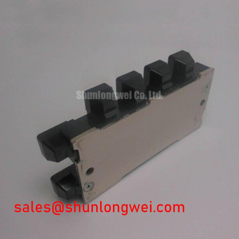
The PM50B6LA060 is identified as a Mitsubishi Electric intelligent power module for industrial power conversion. The actual switching envelope depends on DC-link voltage, gate-drive behavior, load current, cooling conditions, protection timing, and the host inverter topology. These factors should be kept separate from measured operating limits in the finished drive.
For a heavy-duty variable frequency AC motor drive, desaturation protection is evaluated by observing the relationship between gate command, collector-emitter voltage, phase current, and protection feedback. A short-circuit event can produce a rapid rise in collector-emitter voltage while the gate remains commanded on. The protection circuit must distinguish that event from a normal switching transition, wiring noise, diode recovery behavior, or an incorrectly referenced sense signal. The response interval, including any blanking and soft turn-off sequence, must be confirmed against the original module and gate-driver documentation rather than assumed from the IPM category.
Type-I and Type-II short-circuit behavior should be treated as system-level protection conditions. Engineers evaluating a protection response within a microsecond-scale window should capture the gate-emitter signal and the affected power-node waveform with suitable probing technique. The measurement should show whether the protection circuit removes the gate command cleanly, whether the power loop produces an inductive overshoot, and whether the fault signal returns to its expected state after the event. A two-stage soft turn-off strategy can reduce the rate of current interruption and limit additional voltage stress, but its timing and implementation are determined by the gate driver and the surrounding protection circuit.
When a drive trips during acceleration or motor reconnection, inspect the protection feedback path before replacing the module. Look for a floating reference, excessive common-mode movement, damaged isolation components, incorrect gate polarity, or a control board that is issuing overlapping commands. An oscilloscope comparison between the affected phase and a known-good phase is useful because it separates a module-side abnormality from a control-timing or layout problem. Do not interpret a single abnormal voltage reading as proof of an internal failure without checking the complete signal path.
The gate circuit should be examined for resistor damage, cracked solder joints, contamination, and a return path that shares high-current commutation impedance. The auxiliary emitter or control return, where provided by the original module arrangement, should be routed according to the manufacturer’s terminal definition and kept separate from the high-current emitter path. This reduces the chance that emitter inductance and ground bounce will be interpreted as an unintended gate signal.
Bench Tip: Use ESD protection and record cold-state resistance and diode-mode readings before energizing the assembly, then compare each phase leg with the corresponding phase on a known-good board.
For broader gate-drive, thermal, and protection relationships, engineers can consult IGBT Design & Integration as a technical reference. The page should supplement, not replace, the original Mitsubishi Electric data applicable to the PM50B6LA060 installation.
Assembly Integrity & Layout Architecture: Implementing DC-Link Capacitance Bank Layout and Low-ES for PM50B6LA060
Check the DC positive, DC negative, phase-output, and control-terminal connections for correct polarity and mechanical integrity before measuring the switching waveform. A loose busbar joint, uneven mounting surface, or probe ground lead placed across a high-current loop can create readings that do not represent the actual electrical behavior of the PM50B6LA060 assembly.
The DC-link capacitor bank should be positioned and connected so that the commutation loop is short, symmetrical, and mechanically stable. This is a Design Consideration, not an official PM50B6LA060 package specification. The design objective is to reduce parasitic inductance and resistance between the capacitor bank and the module power terminals, limiting turn-off overshoot and reducing unwanted ringing. The peak power-node voltage is influenced by the DC-link voltage, loop inductance, and current-change rate, so the system engineer must verify the resulting peak against the module’s documented electrical limits during switching tests.
Low-ESR capacitors can improve high-frequency current support, but capacitor selection cannot be separated from ripple-current capability, temperature, lifetime requirements, resonance, fuse coordination, and the physical busbar structure. A small high-frequency capacitor may address a local current path while creating a resonance with the larger DC-link bank. Measure the actual network with the intended busbar, capacitor, snubber, and module arrangement in place rather than evaluating one component in isolation.
Symmetrical planar busbar geometry is a useful Design Consideration where multiple phase legs share a common DC link. Keep the forward and return conductors close together and avoid unnecessary loop area. The final clearance and creepage arrangement must be checked against the working voltage, pollution environment, insulation system, enclosure, and applicable equipment standard. Clearance should be checked through air, while creepage follows the surface path and can be affected by contamination, slots, coatings, and material group.
Terminal verification should begin with the original wiring diagram and continue with continuity checks performed without power. Mark each cable by function before removal, inspect crimp barrels and threaded interfaces, and confirm that a control terminal has not been connected to a power terminal through a misplaced harness. A resistance check alone cannot confirm correct switching polarity, so the low-voltage control test should be performed with current limited and with the power stage safely isolated.
Mechanical fastening affects electrical performance. Busbars must remain flat against their intended interfaces, and fasteners should be secured using the assembly procedure specified for the equipment. The mounting surface should be clean and free from burrs that can tilt the module or concentrate mechanical stress. Vibration-resistant fastening is a Design Consideration for industrial drives, but the exact torque, washer arrangement, and thread treatment must come from the applicable Mitsubishi Electric and equipment assembly instructions.
During waveform verification, use a differential high-voltage probe with an appropriate common-mode rating and a short measurement connection. Long oscilloscope ground leads can add inductance and reproduce ringing that is not present at the module terminal. Compare the same test point under no-load, resistive-load, and motor-load conditions where practical, because motor cable length, motor capacitance, and regenerative events can change the observed transient.
Benchtop Waveform Tuning: Mitigating Stress via Optocoupler and Digital Isolation Architectures
Probe the gate-emitter voltage directly at the module terminals and inspect the isolation-side supply and return before adjusting any gate resistor or control timing. A waveform that looks acceptable at the driver board may show overshoot, undershoot, or a false turn-on at the PM50B6LA060 pins because of routing inductance and common-mode movement.
Optocoupler and digital isolation architectures should be evaluated as system alternatives, not treated as interchangeable parts. The relevant checks include propagation delay, delay matching between complementary channels, isolation rating, common-mode transient immunity, output-drive capability, supply decoupling, and behavior during an undervoltage event. Any reinforced isolation requirement must be verified from the selected isolator’s certification data and the complete PCB insulation layout. It is not an inherent rating of the Mitsubishi IPM itself.
Common-mode transient stress can couple through parasitic capacitance between isolated domains and can disturb the gate signal even when the logic command is steady. To investigate a suspected false trigger, observe the input command, isolated output, gate-emitter voltage, and power-node transition on the same time base. A narrow pulse on the isolated output may be caused by insufficient transient immunity, poor return-current control, supply bounce, probe coupling, or an incorrect logic-state relationship. Confirm the cause through repeated measurements under controlled switching conditions.
The gate loop should be compact, with the driver return routed to the appropriate emitter reference rather than through a high-current power path. Where the module provides an auxiliary emitter or dedicated control reference, its use must follow the terminal definition and the original gate-driver topology. Designers should verify whether the existing drive requires a positive-only turn-off state or a negative gate bias; neither should be assumed without the relevant module and driver documentation.
Miller coupling is most visible during the opposing switch transition, when collector-emitter voltage changes rapidly while the gate is near its plateau region. A gate clamp, suitable turn-off impedance, active clamping arrangement, or controlled switching profile may be considered when measured waveforms show excessive gate movement. The selected protection method must be validated against gate-emitter maximum ratings, driver output capability, isolation behavior, and the complete commutation loop.
Bootstrap supplies require separate attention when the gate driver uses a high-side floating channel. Check the bootstrap diode orientation, charging path, capacitor voltage under repetitive switching, refresh interval, leakage, and diode recovery behavior. The required capacitance and voltage margin are determined by gate charge, driver consumption, switching frequency, duty cycle, temperature, and allowable supply ripple. These values are system calculations and should not be presented as fixed PM50B6LA060 specifications.
When the waveform shows a delayed turn-on or an intermittent protection trip, compare the isolated driver supply at the driver pins rather than at the upstream regulator. Inspect decoupling placement, isolation barrier spacing, solder quality, and the return path around the driver. A digital isolator with adequate headline CMTI may still perform poorly if the PCB routes high dv/dt nodes through the isolation boundary or allows a noisy return current to share the control reference.
The Mitsubishi Electric Power Semiconductors and ICs resource provides broader manufacturer-level context for power-device technologies. Selection of an isolator, gate driver, or complementary switching device remains dependent on the original drive design and verified electrical requirements.
Transient Dynamics & Electrical Design: Overvoltage Trip Prevention via Fast Switching
Capture the DC-link voltage during acceleration, deceleration, and fault recovery while simultaneously recording the motor current and brake-command signal. This identifies whether an overvoltage trip is associated with regenerative energy, switching overshoot, an incorrectly timed brake circuit, or a control sequence that leaves the DC link unsupported.
In a heavy-duty variable frequency AC motor drive, deceleration transfers motor kinetic energy back toward the DC link. The braking IGBT and ballast resistor must be selected and controlled so that the available braking path can absorb the expected energy without exceeding the module, resistor, capacitor, or DC-link voltage limits. The required duty cycle depends on motor inertia, speed profile, load torque, braking frequency, resistor thermal behavior, and the drive’s control algorithm. It cannot be inferred solely from the PM50B6LA060 product category.
Check whether the braking path is internal to the drive assembly or implemented with an external switching stage. Verify the brake command polarity, isolation state, gate-drive supply, resistor connection, and fault feedback. A brake circuit that remains off may result from a control interlock, an undervoltage condition, an open resistor path, or a protection latch rather than a failed power module. Measure each condition in sequence and compare it with the equipment’s documented control logic.
Fast switching can reduce switching loss in some operating conditions but can also increase voltage overshoot, electromagnetic coupling, and gate stress. The appropriate switching profile is determined by the measured relationship between current-change rate, loop inductance, gate resistance, snubber behavior, and thermal performance. Engineers should minimize parasitic loop inductance and verify peak voltage margins against the DC-link voltage during switching tests instead of assigning a universal inductance or gate-resistance target to this model.
Snubber evaluation should include capacitor dielectric behavior, pulse-current capability, resistor energy handling, placement, and the resulting resonance. A snubber located far from the switching loop may have little effect at the transition being measured. Conversely, an incorrectly damped network can increase circulating current or create a new oscillation. Use differential probing at the module terminals and compare the waveform with the snubber connected and disconnected only under a controlled, current-limited test arrangement.
Review the DC-link overvoltage threshold against the module’s documented voltage rating and the drive manufacturer’s protection settings. The threshold must leave appropriate room for measurement tolerance, switching overshoot, regenerative rise, and temperature-dependent behavior, but the actual margin is determined by the complete system safety analysis. Do not treat a trip threshold as proof that the module itself has reached its absolute electrical limit.
For field troubleshooting, inspect the motor cable, braking resistor, contactors, precharge circuit, DC-link capacitor condition, current sensors, and control-board event log. Compare the trip waveform with a normal deceleration waveform and check whether the fault appears at a repeatable speed, load, or temperature. This evidence is more useful than assigning a single cause from the alarm code alone. After any power-stage intervention, repeat insulation, polarity, control-signal, and low-voltage functional checks before returning the drive to service.
Use the original Mitsubishi Electric documentation and the equipment service procedure to confirm every terminal function, electrical boundary, protection sequence, and permitted operating condition for the PM50B6LA060 installation.