


Content last revised on October 2, 2026
7MBR10SA120-70 Operational Boundaries: Evaluating Dynamic Braking Chopper Operation Limits
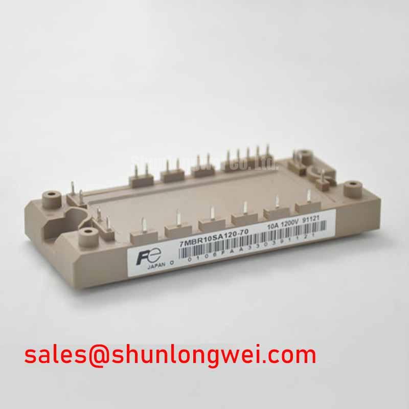
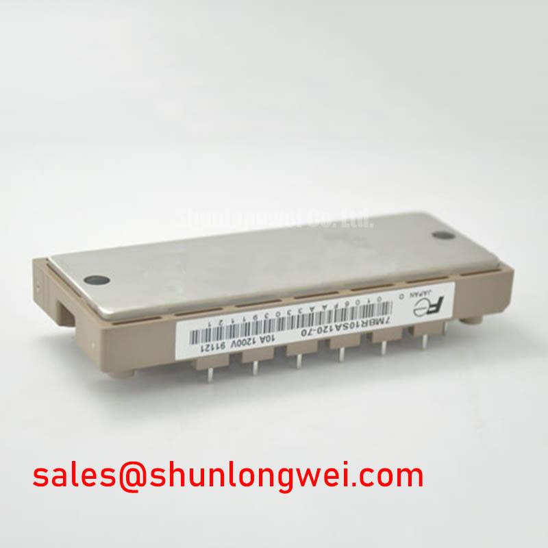
Start the bench check by isolating the drive from the DC link, inspecting the module body and terminals for mechanical damage, and confirming the nameplate boundary of 1200.0 V and 10.0 A before any energized test. The Fuji Electric 7MBR10SA120-70 is a Module type power semiconductor unit listed for evaluation in industrial inverter, braking, and motion control assemblies. The available product data identifies its rated voltage as 1200.0 V and rated current as 10.0 A. Gate terminal arrangement, internal circuit topology, switching ratings, thermal resistance, and isolation specifications should be confirmed from the original Fuji Electric documentation for the exact production variant.
For a stopped light industrial automation system or multi joint robotic articulator, the first useful comparison is normally between the failed unit and a known good phase or braking channel. With power removed and the DC link safely discharged, record cold resistance or diode mode readings between the accessible power terminals and compare the results symmetrically. A single reading should not be treated as a complete diagnosis because connected snubbers, gate driver components, current sensors, and parallel protection paths can influence the measurement. If the module is removed from the circuit, repeat the check at the device terminals and document polarity, meter range, ambient condition, and visible terminal contamination.
When this Fuji Electric module is being assessed for a dynamic braking chopper, the key question is not only whether the semiconductor carries the motor current. The braking branch must also absorb the kinetic energy returned during deceleration without exceeding the device voltage, current, thermal, and switching limits. The braking resistor, DC link capacitor, chopper duty cycle, acceleration profile, and permitted stopping frequency are system-level variables. The 1200.0 V rating is an official product parameter, not a substitute for measuring the actual switching waveform at the module terminals.
During commissioning, measure the DC link voltage at the power stage rather than relying solely on the inverter display. Use a properly rated differential probe and examine the voltage rise when the braking command begins, including the turn off interval of the chopper. Stray inductance in the resistor connection and busbar can create a local overshoot that is absent from a remote control board measurement. Designers should minimize the high current commutation loop and verify the peak voltage against the module rating under the highest expected motor inertia, line condition, and ambient temperature.
The resistor must be evaluated for pulse energy, average dissipation, enclosure temperature, and cooling clearance. A resistor that survives one emergency stop may still overheat during repeated indexing of a robotic axis. The braking controller should be checked for its enable threshold, hysteresis, fault response, and interaction with the main inverter protection. If the chopper repeatedly activates during ordinary motion, investigate regenerative energy, deceleration settings, DC link capacitance, and resistor sizing rather than assuming a semiconductor fault.
For a field replacement, compare the original terminal function, mounting pattern, gate drive connection, and cooling interface before considering any substitute. The 6MBI450U-120A-05 is a separate product that may be reviewed as part of a neutral engineering comparison, but electrical ratings, internal topology, pin assignment, and thermal behavior must be verified before any replacement decision. A different current class or module family should not be treated as a direct substitute based on package appearance alone.
⚠️ Field Alert: Disconnect the supply and verify DC link discharge with an appropriate meter before removing the module or touching gate wiring.
Transient Dynamics & Electrical Design: Auxiliary Emitter Return Trace Separation on 7MBR10SA120-70
Gate drive instability is often investigated after a module passes a static diode check but fails during switching. If the installed circuit provides a separate auxiliary emitter or driver return, the system designer should determine whether that return is intended to carry only the gate drive reference or shares copper with the high current emitter path. Shared impedance can feed switching voltage back into the driver reference and create apparent gate ringing, delayed turn off, or an unexpected protection trip.
The practical method is to inspect the complete current loop on the board and busbar, then probe the gate to its correct emitter reference directly at the module terminals. A probe connected to a distant control ground can display a waveform that is dominated by measurement loop inductance. Compare turn on and turn off behavior at the lowest validated operating point before increasing switching stress. The gate resistor, driver output impedance, isolated power supply, clamp network, and any Miller control circuit should be reviewed as one system.
Minimizing parasitic gate loop inductance is a design consideration for suppressing oscillation, but the suitable damping value is determined by the driver, gate charge, layout, switching speed, and measured waveform. Engineers should tune the circuit while checking gate overshoot, negative excursion, collector or drain voltage, and current commutation at the actual module terminals. No universal gate resistor or negative gate bias should be assigned to this model without the relevant Fuji Electric switching data and the driver schematic.
Switching frequency also changes the thermal result. A design that appears stable at a low pulse rate may develop excessive junction temperature during sustained high frequency operation because switching losses accumulate even when the average motor load is moderate. For a robotic axis, review the real motion profile, dwell time, braking events, airflow path, heatsink contact, and cabinet temperature. The thermal network should be evaluated with the manufacturer’s transient thermal impedance information when available. Short current pulses, repetitive braking pulses, and continuous PWM should not be represented by one simplified temperature estimate.
If oscillation appears only after the cabinet is closed, compare the open cabinet and installed airflow conditions while maintaining safe operating limits. Check whether cable routing has changed the gate return loop or placed the gate wiring beside a high dv/dt conductor. The Fuji Electric Power Semiconductors Portal provides the appropriate manufacturer product context; the exact 7MBR10SA120-70 switching and gate information should be matched to the original technical documentation.
7MBR10SA120-70 Thermal-Electrical Optimization: High-Altitude Cosmic Ray Induced SEB Failure Practical Tuning
High altitude and single event burnout require careful source control because the available product data for this page does not provide a device specific FIT value, SEB probability, altitude derating curve, or guaranteed DC bus reduction. These figures must not be inferred from the 1200.0 V voltage rating. A design review for equipment installed above ordinary industrial elevations should obtain the applicable manufacturer reliability information and evaluate the complete operating environment, including DC link voltage, switching transients, cooling condition, enclosure altitude, and duty cycle.
As a design consideration, higher altitude can affect cooling because air density and enclosure heat rejection change with installation conditions. The system engineer should verify the actual heatsink temperature and module case temperature during the most demanding motion and braking sequence. A temperature estimate based only on room temperature can miss local heating at the module baseplate, resistor, busbar, or driver board. The thermal interface should be inspected for even contact, contamination, mounting flatness, and correct fastener practice according to the assembly documentation.
For a suspected high energy failure, preserve the failed assembly before cleaning or removing surrounding components. Record the DC link condition, fuse or breaker response, gate driver fault history, braking resistor condition, and any damage on adjacent copper. Then test the driver output without reconnecting a replacement power module until abnormal command pulses and supply behavior have been checked. A failed module may be the result of an upstream overvoltage, gate drive fault, inadequate commutation layout, or thermal event; the visual failure point alone does not establish the initiating mechanism.
Designers reviewing cosmic ray or SEB exposure should use a documented reliability method rather than applying an unsupported FIT multiplier. The DC bus margin, switching overshoot, installation altitude, and semiconductor technology must be evaluated together, and any proposed derating must be validated through the relevant manufacturer or standards based evidence. The Ultimate IGBT Knowledge Base can provide broader technical background, while model specific decisions still require the applicable Fuji Electric data.
7MBR10SA120-70 Operational Boundaries: Evaluating Common Mode Transient Immunity in Harsh Limits
The 7MBR10SA120-70 product information supplied here confirms the module category, 1200.0 V voltage rating, and 10.0 A current rating. It does not confirm a reinforced isolation voltage, a common mode transient immunity value, or a specific gate driver architecture. Those characteristics belong to the complete drive assembly or to separately documented components. A module should therefore not be described as independently certified for an isolation or EMC requirement that applies to the finished equipment.
When a robotic axis shows intermittent gate faults, inspect the isolation barrier, driver supply decoupling, control cable shielding, connector seating, and physical separation between power switching nodes and logic traces. Use an oscilloscope with suitable common mode measurement practice to compare the command signal at the driver input with the gate to emitter waveform at the module. A false trigger may be associated with capacitive coupling, reference movement, insufficient driver supply stability, or an incorrect probing method. The measured waveform and the known good channel should guide the next test rather than a single assumed cause.
For harsh switching environments, keep the gate command loop compact and route the power return separately from sensitive control references where the circuit architecture permits. The system integrator should verify creepage, clearance, insulation coordination, connector spacing, and enclosure contamination requirements against the working voltage and applicable equipment standard. Layout decisions must also account for the real busbar geometry and switching edge rate; a nominal schematic separation does not prove adequate transient performance.
The Fuji Electric PIM 7-Pack information is useful for understanding the manufacturer’s broader power module portfolio, but it should not be used to infer unlisted specifications for this exact model. Before energizing a replacement in a multi joint robotic articulator, verify terminal identity, driver polarity, protection timing, cooling contact, and the measured DC link waveform under controlled commissioning conditions.