Content last revised on September 15, 2026
Preventing Spurious Faults: FIT and High Altitude Evaluation for PM50RHA060
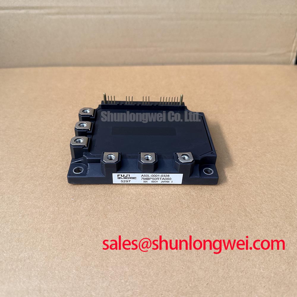
Before fitting a replacement, isolate the drive, verify the nameplate against PM50RHA060, and confirm that the controlled DC bus cannot exceed the module’s 600 V VCES official rating during normal operation or switching transients. Mitsubishi Electric specifies this power module at 50 A continuous collector current with case temperature at 25°C, 100 A peak collector current for 1 ms, 125 W collector dissipation per IGBT, and a typical 1.8 V VCE(sat) at 50 A and 25°C. The official minimum short circuit withstand time is 10 μs. These values define the device boundary; they do not replace measurements of the installed inverter, cooling path, gate drive, or protection response.
| Official Datasheet Specification | Value |
|---|---|
| Collector Emitter Voltage, VCES | 600 V |
| Continuous Collector Current, IC, TC = 25°C | 50 A |
| Peak Collector Current, ICP, 1 ms | 100 A |
| Collector Dissipation per IGBT, TC = 25°C | 125 W |
| Collector Emitter Saturation Voltage, VCE(sat) | 1.8 V typical at 50 A, 25°C |
| Short Circuit Withstand Time, tsc | 10 μs minimum |
The PM50RHA060 is rated by Mitsubishi Electric for a 600 V collector emitter blocking condition, but a DC bus rating alone does not establish the actual voltage stress at the semiconductor terminals. During turn off, the voltage seen by the IGBT is affected by commutation current, switching speed, busbar inductance, cable routing, capacitor placement, diode recovery behavior, and measurement technique. A meaningful commissioning check uses a suitably rated differential voltage probe and current probe to observe collector emitter voltage at the module connection points while the drive operates through its intended load range.
High altitude evaluation needs particular care because terrestrial neutron flux, cooling performance, enclosure pressure, and insulation coordination can all be system dependent. No PM50RHA060 specific FIT value, single event burnout rate, altitude rating, or cosmic ray derating curve is included in the supplied official specifications. It would therefore be inappropriate to calculate or publish a numeric FIT prediction for this module. Design Consideration: where equipment will operate above 2000 m or in another location with altered environmental conditions, the equipment designer should obtain the applicable site, insulation, thermal, and reliability requirements, then validate the DC bus headroom and protection behavior under representative electrical stress.
A nuisance overcurrent trip, unexpected desaturation event, or repeated collector voltage overshoot can arise from several interacting causes. Begin by confirming the actual DC link voltage, probe grounding arrangement, current sensor polarity, gate command overlap, and the physical location of DC link capacitors. Then compare the affected phase against a known good phase using the same probe placement. An apparent overshoot that changes substantially when probe grounding changes may be a measurement artifact rather than a device condition. A repeatable difference between phases can point toward unequal commutation loops, degraded bus connections, a gate driver problem, or an external load fault.
The official 10 μs minimum short circuit withstand time is a protection coordination boundary, not a permitted recurring operating interval. The controller, sensing method, gate driver shutdown path, and DC source impedance determine whether a real fault is cleared appropriately. Engineers investigating a fault should capture the interval between fault onset and gate removal, then verify that the test arrangement does not expose the module to repeated uncontrolled fault pulses. For broader selection and system reliability context, see the Power Electronics Masterclass.
PM50RHA060 Thermal Electrical Optimization: Derating and Parameter Mismatch Tuning
The 1.8 V typical VCE(sat) figure is an official test value at 50 A and 25°C, not a maximum loss figure for every load point or temperature. Conduction loss changes with current, junction temperature, modulation pattern, and the operating duty cycle. The stated 125 W per IGBT collector dissipation is also specified at a 25°C case temperature. In a practical drive, the case temperature is established by heatsink performance, interface condition, airflow, enclosure temperature, and the heat generated by adjacent power devices. Thermal assessment should therefore use measured case temperatures and the original equipment thermal design rather than treating the 25°C rating condition as the normal field environment.
When parallel current paths or complementary switching devices are involved, the positive temperature tendency of IGBT saturation voltage can support steady state current sharing under suitable matched conditions. It does not ensure dynamic sharing during fast transitions. Dynamic imbalance is commonly influenced by unequal gate resistance, unequal driver return paths, different stray inductance, or physically different connection lengths. Design Consideration: keep corresponding gate command and return loops geometrically similar so that each switching position sees comparable parasitic impedance, then confirm current and voltage behavior using switching measurements.
Dead time and gate interlock must be determined by the complete inverter. The relevant conditions include actual turn off propagation delay, gate discharge behavior, temperature, reverse recovery of the commutating path, controller timing tolerance, and noise immunity. A dead time setting that is too short can permit cross conduction, while excessive dead time can distort current control and increase loss elsewhere in the power stage. The system engineer should verify both complementary gate signals at the driver outputs and the module terminals, particularly during command transitions, regenerative conditions, and startup sequences.
Integrated robotic articulator drives and light industrial automation axes can produce frequent acceleration and deceleration transitions. That operating pattern makes a measured loss profile more useful than a current label alone. Check phase current balance, heatsink temperature distribution, commanded switching behavior, and DC link ripple under the actual motion sequence. If a hardware replacement study is required, the CM100DY-12E can be reviewed as a separate candidate, but its electrical ratings, connection arrangement, driver compatibility, thermal interface, and protection timing must be verified against the original design before any substitution decision.
Preventing Spurious Faults: Planar Symmetrical Busbar Geometry for PM50RHA060
Turn off voltage stress follows the familiar relationship in which peak voltage is influenced by DC bus voltage plus the product of loop inductance and current slew rate. This is an engineering principle, not a PM50RHA060 specific transient limit. The module’s official 600 V VCES rating remains the boundary to protect, while the actual peak must be measured in the assembled converter. Compact planar conductor geometry, close placement of the DC link capacitor, and short commutation paths help reduce parasitic loop inductance and therefore reduce inductive overshoot.
Do not apply a generic inductance target or snubber value to this module without testing. Snubber selection depends on measured ringing frequency, loop inductance, operating current, switching frequency, capacitor characteristics, and the intended loss budget. The appropriate method is to identify the commutation loop, measure collector emitter waveform and current at relevant operating conditions, and evaluate whether the observed peak retains suitable margin to the official voltage rating. The final component values and physical geometry are system determined and should be validated on the completed power assembly.
Reverse recovery behavior of the freewheel path can influence the switching current waveform, voltage ringing, and radiated or conducted noise. A reverse recovery softness factor is not included in the supplied PM50RHA060 official data, so no numerical softness claim should be assigned to this part. Where recovery related ringing is suspected, capture the current reversal and collector voltage together. Compare switching events in motoring and regeneration, as the current direction and commutation path can change the waveform. A result that is only visible on one phase should prompt inspection of that phase’s capacitor connection, conductor spacing, gate routing, and driver return reference.
💡 Pro Tip: Route each commutation path as a compact, symmetric supply and return pair, then verify the actual turn off peak at the module terminals with a correctly connected differential probe.
Clearance and creepage requirements belong to the complete assembly, including bus voltage, pollution degree, enclosure construction, terminals, and applicable end equipment standards. They should not be inferred from this module’s voltage rating alone. In systems where an upstream rectifier or another power stage is being assessed as part of the same repair, the CM300DXDX1-24A is a related power module that can be considered within the wider topology review, subject to independent electrical and mechanical verification.
PM50RHA060 Operational Boundaries: Evaluating High dv/dt Cross Conduction and Shoot Through Limits
A fast collector voltage transition can couple energy through the IGBT’s effective gate collector capacitance and disturb the gate emitter voltage of the noncommanded switch. The resulting Miller effect can become more significant when the gate return path is inductive, the driver output is weak during off state, or the complementary power loop is physically unbalanced. This mechanism should be checked at the gate emitter terminals, not only at the controller logic output, because the voltage at the module is what determines switching behavior.
For PM50RHA060 integration, inspect whether the driver maintains a defined off state throughout the opposing switch’s transition. An active Miller clamp or a suitably designed low impedance off state path can be evaluated as a Design Consideration when measured gate disturbance indicates cross conduction risk. The required gate bias strategy must come from the original gate driver documentation, module documentation, isolation ratings, controller sequencing, and test results. A fixed negative gate bias value should not be assumed from generic IGBT guidance.
Mitsubishi Electric’s DIPIPM™ Bootstrap Circuit Design note offers useful reference material on high side supply and switching circuit considerations. It should be read as application guidance rather than as a PM50RHA060 specific gate drive specification. Likewise, Mitsubishi Electric’s power semiconductor device resources can support a wider review of power module operating conditions.
A structured troubleshooting sequence begins with the DC bus disabled and the equipment safely discharged. Verify gate driver supply integrity, complementary command timing, driver enable logic, current sensing, and phase output connections. Under controlled powered testing, compare the gate emitter voltage of each relevant switching position against the associated collector voltage transition. Evidence of gate lift, unexpected overlap, or unequal waveform ringing may indicate an interaction between driver impedance, layout inductance, sensor behavior, or external load conditions. The corrective action should be selected only after the complete switching event has been observed and assessed against the PM50RHA060 official electrical limits.