Content last revised on September 10, 2026
PCB Gate Loop Layout Symmetry & Kelvin Emitter Routing Rules
In high-power commercial and industrial (C&I) Battery Energy Storage System (BESS) power conversion systems (PCS), power module layout integrity dictates switching fidelity. The Mitsubishi Electric CM300DXDX1-24A dual IGBT module features a rated collector-emitter breakdown voltage of VCES = 1200V and a continuous collector current rating of IC = 300A at TC = 90°C. Managing high current slew rates (di/dt exceeding 3000 A/µs during hard turn-off) requires absolute segregation between the auxiliary Kelvin emitter terminal and the primary power emitter return path.
When high-frequency load current traverses the parasitic inductance of the main power emitter path, any shared trace with the gate drive circuit induces a counter-electromotive force, calculated as:
Vinduced = -Lemitter × (diC / dt)
This unwanted feedback lowers the effective gate-to-emitter voltage VGE during turn-on and induces destructive gate voltage oscillations during turn-off. To eliminate emitter mutual inductive coupling, the gate drive PCB traces must connect directly and exclusively to the dedicated auxiliary Kelvin emitter pin of the module. Drive loops must be routed as tightly coupled differential pairs (or microstrip topologies with minimal loop area) to minimize stray loop inductance Lsigma. Considering the typical total gate charge of QG = 1350 nC (at VCC = 600V, IC = 300A, VGE = 15V), driver stages must supply peak gate currents according to:
IG(peak) = (VGE(on) - VGE(off)) / (RG(int) + RG(ext))
Maintaining symmetrical gate traces across both high-side and low-side switches inside the dual pack ensures identical switching behavior and uniform dynamic stress.
Multi-Module Parallel Current Sharing & Positive Tempco Balancing
Scaling PCS capacity into the megawatt range requires paralleling multiple IGBT modules across common DC-link and AC-bus structures. Static and dynamic current sharing across paralleled CM300DXDX1-24A devices depends on semiconductor material properties and structural busbar symmetry.
| Parameter | Symbol | Rated Value | Test Conditions | Impact on System Architecture |
|---|---|---|---|---|
| Collector-Emitter Saturation Voltage | VCE(sat) | 2.0 V (typ) / 2.6 V (max) | IC = 300 A, VGE = 15 V, Tj = 25°C | Positive temperature coefficient stabilizes steady-state static current sharing across paralleled modules. |
| Thermal Resistance (Junction-to-Case) | Rth(j-c) | 0.078 K/W (max, IGBT) | Per switch, TC measured directly under silicon die | Governs thermal dissipation limits into the liquid-cooled cold plate. |
| Internal NTC Thermistor | RNTC | 5 kΩ (typ) | T = 25°C, B(25/50) = 3375 K | Provides localized baseplate temperature feedback for overload limiting. |
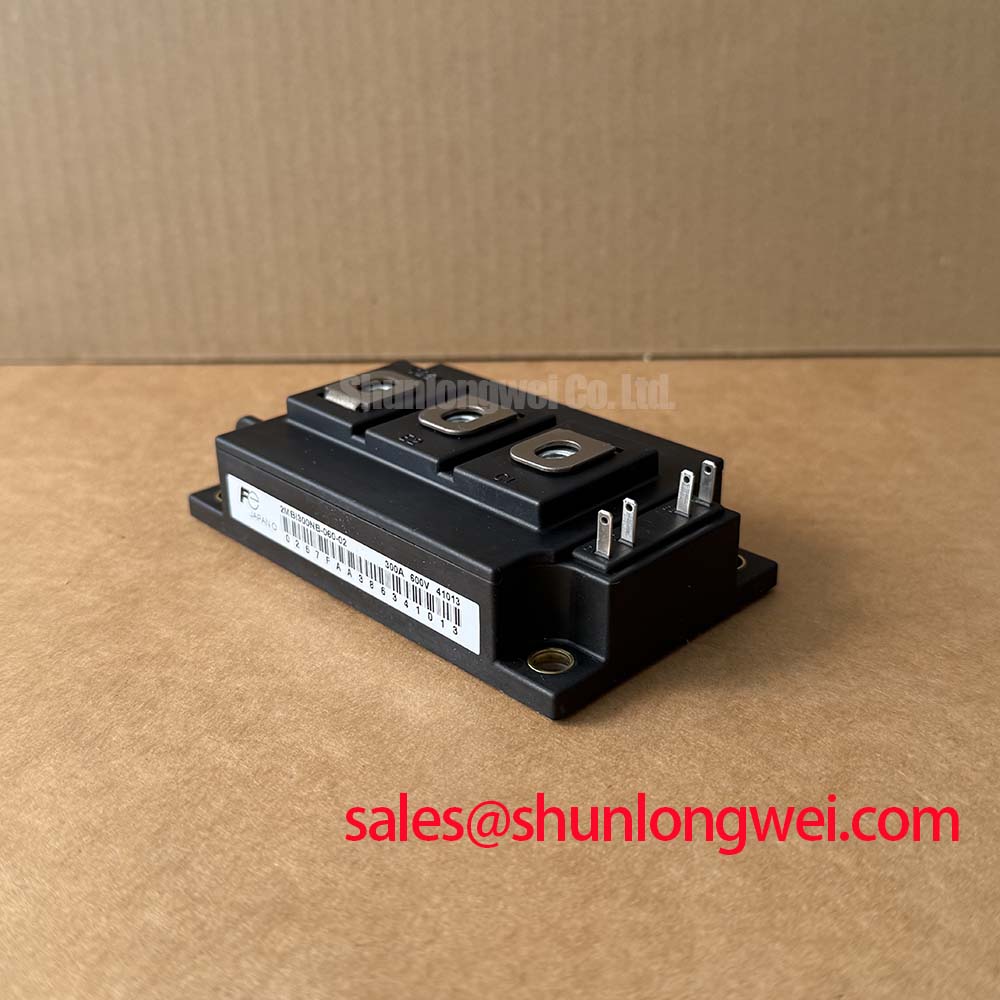
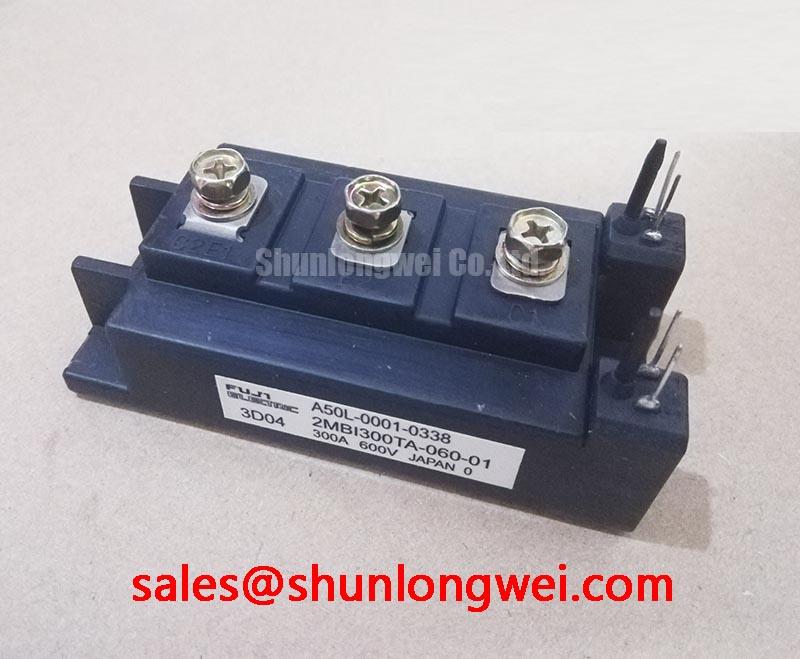
The CM300DXDX1-24A exhibits a positive temperature coefficient of saturation voltage at nominal currents. When an individual module draws more current, its junction temperature Tj rises, leading to an increase in VCE(sat). This automatic self-regulating mechanism shifts current to cooler, paralleled modules during continuous conduction. For alternative power architectures utilizing 600V platforms or legacy drive hardware, the 2MBI300J-060 provides a benchmark for evaluating 300A dual-switch conduction losses under lower DC-bus constraints.
Dynamic current distribution during the switching intervals cannot rely on the positive thermal coefficient. Parasitic busbar inductances and gate timing skews dominate transient sharing. Symmetrical planar laminations for the DC busbars are mandatory to equalize stray inductance across all parallel branches.
Active Miller Clamp Implementation & Parasitic Turn-On Prevention
In high-voltage half-bridge topologies operating at 600V to 850V DC-link levels, steep collector-emitter voltage transients (dv/dt) on the switching node can trigger shoot-through faults in the complementary switch. When the lower IGBT turns on, the rising voltage across the upper IGBT generates a displacement current through its parasitic collector-gate Miller capacitance Cres (CGC):
idisp = CGC × (dvCE / dt)
This current flows through the internal and external gate turn-off resistance, producing a positive voltage spike at the IGBT gate:
VGE(induced) = idisp × (RG(int) + RG(ext)) + VGE(off)
If VGE(induced) exceeds the gate threshold voltage VGE(th), spurious turn-on occurs, resulting in hazardous cross-conduction current spikes. To prevent this, designers must deploy gate driver ICs featuring an Active Miller Clamp (AMC) or provide negative gate bias (-5V to -15V). The active clamp continuously monitors the gate node; once the gate voltage falls below a set threshold (typically +2.0V) during turn-off, an internal low-impedance MOSFET clamps the gate directly to the negative rail, shunting the displacement current away from the main gate resistor.
As switching speeds scale in next-generation converter designs—highlighted by advancements in Mitsubishi Electric SiC Power Modules & SBDs—controlling dv/dt-induced gate bounce becomes a fundamental requirement for maintaining functional reliability in high-density power electronic conversion.
Bi-Directional DC-DC Buck-Boost Conversion & Battery Cycling Thermal Management
In C&I BESS PCS designs, the CM300DXDX1-24A serves either in the three-phase AC/DC active front end (AFE) or in bi-directional DC-DC buck-boost stages linking battery racks to the DC bus. Battery energy storage involves cyclic operating profiles: long charging periods at constant current, followed by rapid, high-current discharge during peak-shaving operations.
These dynamic load variations expose the power module to thermal cycling stress (ΔTj), stressing the internal bond wires and substrate solder interfaces. Total power loss per switch Ptotal is computed as the sum of static conduction losses and dynamic switching losses:
Ptotal = (1/T) ∫ (VCE(sat) × iC(t)) dt + (Eon + Eoff) × fsw
The resulting junction temperature rise is governed by the thermal path through the module baseplate and thermal interface material (TIM):
Tj = Tambient + Ptotal × (Rth(j-c) + Rth(c-s) + Rth(s-a))
With an Rth(j-c) maximum of 0.078 K/W for the IGBT section, thermal resistance must be tightly controlled via proper mounting torque and void-free TIM application. In discrete buck or boost legs where single switches are deployed alongside complementary freewheeling paths, devices such as the 1MBI300L-060 are frequently examined to model thermal stress distributions in isolated power stages. For detailed validation standards, thermal cycling limits, and lifetime prediction models across industrial IGBT installations, refer to the methodologies outlined in the Field Engineer’s Handbook.