Content last revised on September 10, 2026
Optocoupler vs Digital Coreless Transformer Isolation in High-Voltage Switching
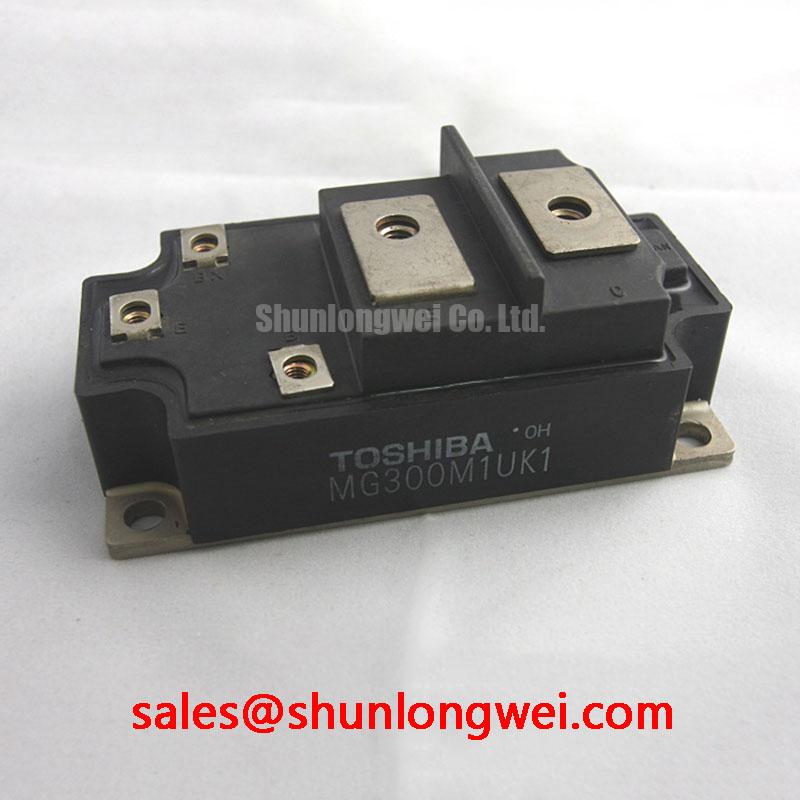
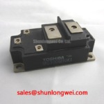
Incoming quality verification of high-power switching stages requires strict isolation barrier evaluation, especially in commercial string inverters and battery energy storage converters. The Toshiba MG300M1UK1 power module is rated at a maximum collector-emitter voltage of VCES = 1000V (Official Datasheet Specification) with a continuous collector current capability of IC = 300A (Official Datasheet Specification). In transformerless grid-tied topologies, switching nodes experience severe ground potential shifts during rapid commutations.
When bench-testing the incoming driver stage paired with the Darlington-configured MG300M1UK1, galvanic isolation integrity determines gate stability. Standard optocouplers offer internal physical separation, but aging LED emission efficiency and package creepage can degrade common-mode transient immunity. Digital coreless transformer isolation provides robust CMTI performance exceeding 100 kV/µs, preventing phantom turn-on events caused by fast dv/dt transients.
💡 Bench Tip: Before connecting drive signals to the high-impedance base/gate terminals, perform cold-state continuity and junction verification using a calibrated digital multimeter in diode-check mode. Verify that the auxiliary emitter and control inputs exhibit standard forward thresholds without leakage to the isolated baseplate, avoiding electrostatic discharge (ESD) degradation during handling.
Layout clearance between primary logic lines and floating secondary channels must maintain a minimum physical creepage distance of 8.0 mm (General Industry Design Consideration for 1000V working insulation). For system evaluations spanning lower current stages, engineering teams comparing module specifications can reference the MG20G6EL1 as an alternate design point within compact industrial layouts.
Managing High-C-Rate Battery Cycling Swings via Symmetrical DC-DC Switching
Commercial energy storage interfaces demand bi-directional four-quadrant power flow to manage heavy charge and discharge C-rates. The MG300M1UK1 features a maximum collector-emitter saturation voltage of VCE(sat) = 2.5V (Official Datasheet Specification) and a DC current gain of hFE = 100 (Min) (Official Datasheet Specification). Conduction losses during aggressive peak-shaving cycles generate substantial localized heat, demanding predictable thermal management.
The module exhibits a low junction-to-case thermal resistance of Rth(j-c) = 0.078 °C/W (Official Datasheet Specification), functioning within a maximum junction temperature rating of Tjmax = 125 °C (Official Datasheet Specification). In bi-directional buck-boost battery balancers, thermal stress oscillates proportionally with load step-changes. Symmetrical phase-angle control distributes conduction profiles across complementary pairs to prevent localized junction hotspots.
| Parameter | Official Specification | Engineering Significance |
|---|---|---|
| Collector-Emitter Voltage (VCES) | 1000V | Voltage ceiling for industrial DC buses & grid inverters |
| Collector Current (IC) | 300A | Current handling for high-capacity motor drives & storage |
| Collector-Emitter Saturation Voltage (VCE(sat)) | 2.5V (Max) | Defines primary conduction loss during on-state stages |
| Junction-to-Case Thermal Resistance (Rth(j-c)) | 0.078 °C/W | Defines heat extraction rate from semiconductor dies |
| DC Current Gain (hFE) | 100 (Min) | High amplification minimizes driver-stage input loading |
| Maximum Junction Temperature (Tjmax) | 125 °C | Absolute upper thermal boundary for reliable operation |
Advanced thermal dissipation designs often integrate Heat Pipe Phase-Change Cooling in High Power Electronics to transport heat away from high-power footprints. Applying a uniform thermal interface material layer of 50 to 100 µm thickness (Typical Starting Point for bench tuning) ensures minimal interface resistance across the module baseplate.
High-Frequency Commutation Loop Inductance Minimization in High-Power Arrays
During turn-off under heavy collector current loads, parasitic inductance within the DC-link commutation loop generates transient overvoltage spikes across the main terminals. When commutating a 300A rail, total turn-off peak voltage follows the combined dynamic profile where peak terminal stress is the sum of the DC-link potential and the induced Lσ × (di/dt) transient voltage drop.
⚠️ Field Alert: Excess busbar loop inductance (Lσ > 40 nH) can drive turn-off voltage transients beyond the rated 1000V VCES limit when clearing overcurrent conditions. Engineers must place low-inductance polypropylene film snubber capacitors directly across the module's positive and negative terminals, targeting a total stray commutation inductance under 25 nH (General Industry Design Consideration for high-power switching assemblies).
Planar laminated busbars using overlapping copper plates separated by thin dielectric films such as Polyether Ether Ketone (PEEK) High Durability Polymers in Harsh Environments reduce loop area and cancel opposing magnetic fields. In bench quality evaluations, verify snubber capacitor ESR and ESL via impedance analyzers prior to running dynamic commutations.
PCB Gate Loop Layout Symmetry & Kelvin Emitter Routing Optimization
To avoid gate oscillation and false re-triggering during aggressive di/dt switching transitions, layout routing must completely isolate control circuits from high-current power return paths. The Toshiba MG300M1UK1 incorporates auxiliary emitter terminals designated specifically for driver return reference.
Connecting the gate driver reference directly to the power emitter busbar introduces severe inductive ground bounce into the control circuit. By routing a dedicated Kelvin emitter trace from the auxiliary emitter directly back to the gate driver return, base/gate drive signals remain unaffected by main power path inductance.
Bench validation procedures must encompass static leakage screening, dynamic signal logging, and baseplate insulation verification. For deep technical testing methodologies and screening protocols, consult the comprehensive Field Engineer’s Handbook for standardized failure analysis workflows.
Maintain tight twisted-pair or differential PCB track routing for gate and Kelvin emitter traces with a loop area below 1.5 cm² (Typical Starting Point for noise-immune driver design), minimizing stray electromagnetic pickup from neighboring magnetic components.