
Content last revised on November 6, 2026
MG300J2YS45 Identification and Installation Checks
- Isolate the power supply, verify DC-link discharge, and compare cold terminal measurements with the equipment schematic before disconnecting the MG300J2YS45.
- Inspect the heatsink contact surface, mounting threads, and existing thermal compound for uneven contact, contamination, or displacement.
- Trace the gate and emitter return connections to the driver board, checking connector condition and separation from the main switching conductors.
- Record cooling airflow, terminal discoloration, and evidence of condensation so that replacement work addresses the surrounding operating conditions.
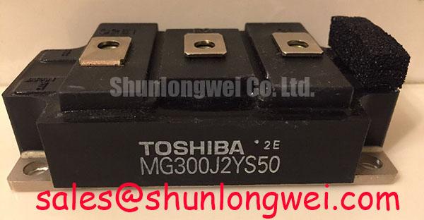
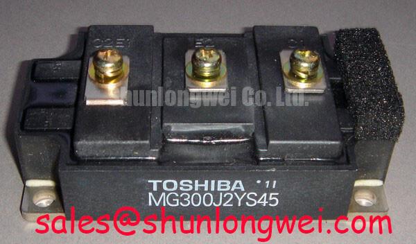
The MG300J2YS45 is a Toshiba IGBT Module with a collector-emitter voltage rating (VCES) of 600.0 V and a collector current rating (IC) of 300.0 A under the specified datasheet conditions. These electrical ratings provide the starting point for identifying the power stage; installation assessment also requires matching the original circuit connections, mechanical interfaces, and gate-drive requirements.
| Specification | Product value |
|---|---|
| Manufacturer | Toshiba |
| Part Number | MG300J2YS45 |
| Product Category | IGBT Module |
| Collector-Emitter Voltage Rating (VCES) | 600.0 V |
| Collector Current Rating (IC) | 300.0 A under the specified datasheet conditions |
| Package | Toshiba Module |
| Configuration / Topology | IGBT Power Stage |
| Installation-specific specifications | Consult Datasheet for terminal assignments, mounting requirements, gate limits, thermal characteristics, and rating test conditions. |
The product values above identify the specified hardware. The integration and maintenance guidance below is classified as Design Consideration, rather than additional manufacturer specifications. For equipment compatibility assessment, engineers may evaluate this module for electric material handling equipment and forklift traction converters, subject to the original controller topology, battery operating range, regenerative operation, and cooling arrangement.
MG300J2YS45 Thermal-Electrical Optimization: Thermal Paste Degradation Prevention
Remove residual thermal compound from the module contact face and heatsink using a cleaning method compatible with both surfaces, then inspect the seating area before applying fresh material. Raised debris, damaged threads, and local surface distortion can prevent uniform contact even when the mounting hardware appears secure. Preserve the original mounting orientation and compare the seating condition with the equipment assembly drawing.
As a Design Consideration, control thermal interface thickness through the selected compound’s application procedure and the approved mounting method. The objective is to fill surface irregularities while avoiding an unnecessarily thick thermal path. A uniform application pattern and a controlled trial fit can help reveal incomplete coverage. Inspecting the contact imprint during a trial assembly provides useful evidence of voids, edge accumulation, or an uneven seating pattern.
Check baseplate and heatsink flatness against their respective mechanical requirements. Thermal compound accommodates surface texture; substantial curvature requires evaluation of the mechanical interface. Adding more paste does not establish acceptable contact across a distorted mounting surface. Where seating remains uneven, investigate the heatsink, mounting supports, and fastener engagement before returning the assembly to service.
Follow the documented tightening sequence and torque using a calibrated tool. Progressive tightening helps distribute clamping load without pulling one corner down prematurely. Keep electrical terminal tightening separate from baseplate installation: each connection has its own mechanical requirement, and attached busbars should meet the terminals without forcing the module into alignment.
For preventive maintenance, relate inspection frequency to actual contamination, operating hours, thermal cycling, and temperature trends. Clean obstructed fins and filters, check fan operation, and compare case or heatsink temperature at comparable load and ambient conditions. Rising temperature can have several causes, including restricted airflow, interface deterioration, or changed operating losses. Record the measurement location so that later readings remain comparable.
⚠️ Maintenance Note: Monitor terminal temperature rise and cooling airflow during scheduled inspections, and verify tightening requirements before disturbing electrical connections.
After shutdown in a humid environment, inspect for condensation before energizing the gate driver. Enclosure ventilation and environmental controls should follow the equipment requirements. Record thermal compound replacement with the service date, material identification, and seating observations so that subsequent maintenance decisions use the assembly’s condition rather than an invented service interval.
MG300J2YS45 Circuit Protection & Reliability: Gate Drive Resistance Calibration
Compare the existing turn-on and turn-off gate paths before changing external gate resistance around the MG300J2YS45. Record resistor markings, steering diode orientation, driver output capability, and the route of the emitter return. A resistance value copied from another assembly can produce different switching behavior when driver impedance, wiring inductance, or the replacement device’s gate characteristics differ.
As a Design Consideration, assess switching transitions under controlled operating conditions and adjust resistance only within an approved commissioning procedure. Increased gate damping can reduce transition speed and ringing while increasing switching energy. Faster switching can reduce transition losses while raising overshoot and interference. The appropriate balance depends on measured collector-emitter voltage, gate-emitter voltage, current transitions, and the resulting thermal behavior.
Use probes suitable for the switching voltage and measurement location, with connections that minimize measurement-loop pickup. Compare turn-on and turn-off separately; separate gate resistors allow different behavior in each direction where the driver circuit supports that arrangement. Record test conditions alongside waveform captures so that a change in load or temperature is not mistaken for an improvement caused by the resistor adjustment.
Where the existing high-side driver uses a bootstrap supply, assess capacitor charge against gate charge, driver quiescent consumption, leakage, and the longest interval without recharge. Allowable supply droop, capacitor tolerance, temperature behavior, and the available recharge path determine the final selection. Check the floating supply during the operating sequence that creates its greatest charge demand, including startup and extended high-side conduction where applicable.
Desaturation protection also requires coordination with switching behavior. On-state collector-emitter voltage monitoring can identify an abnormal operating condition, but the sensing network, blanking interval, and driver propagation delay influence its response. Review fault turn-off against the applicable short-circuit safe operating area. Controlled soft turn-off can reduce inductive overshoot during a fault; its timing and strength belong to the validated protection design.
For maintenance purchasing comparisons, MG100J6ES52 is a separate device to assess against the original requirements. Its identification alone establishes no interchangeability with MG300J2YS45. A replacement review should compare circuit configuration, terminal mapping, electrical limits, mounting geometry, and switching characteristics before any substitution decision.
MG300J2YS45 Circuit Protection & Reliability: Dynamic Gate Impedance Control
Measure the off-state gate-emitter waveform while the opposing switch commutates to assess susceptibility to unintended turn-on. Collector voltage transitions couple current through the gate-collector capacitance, and impedance in the gate return can convert that current into a gate voltage excursion. Evaluate the waveform at the device connections, with attention to probe placement and the difference between the driver reference and power emitter potential.
As a Design Consideration, an active Miller clamp provides a local discharge path when the device is commanded off. Its effectiveness depends on clamp activation behavior, connection inductance, and current capability. Place the clamp connection and its return so that the disturbance current follows a compact path. Check their relationship to the main gate resistor; a clamp routed through excessive common impedance can lose much of its intended benefit.
Negative gate bias is another system design option, subject to the device gate limits and the driver’s operating requirements. Evaluate the complete gate waveform, including negative undershoot, supply startup, and fault recovery. The selected bias must remain acceptable through tolerances and switching transients. It should come from the validated driver design rather than a generic voltage recommendation.
Trace the driver return separately from the high-current emitter connection wherever the documented terminal arrangement permits. If the assembly provides a dedicated auxiliary emitter terminal, use its assigned function to reduce shared power-path impedance. This routing principle does not establish that MG300J2YS45 includes a Kelvin emitter connection; terminal functions follow the module drawing. Keep gate wiring away from collector switching conductors and retain the equipment’s required insulation spacing.
Suspected cross-conduction warrants comparison of gate commands, actual gate voltages, and current timing. Command overlap, common emitter inductance, driver supply disturbance, and capacitive coupling can produce related symptoms. Establish which mechanism is present before changing dead time or gate components. Repeated resistance adjustments without that distinction can shift losses while leaving the initiating disturbance unresolved.
During maintenance, inspect driver connectors and return-path joints for deterioration that could alter impedance. After a protection trip, capture the relevant supply and gate behavior during an approved diagnostic sequence. Review fault latching and restart control so that a shutdown event does not lead to uncontrolled repeated switching attempts.
MG300J2YS45 Circuit Protection & Reliability: DC-Bus Low-Inductance Laminated Busbar Design
Keep the commutation path between the local DC-link capacitor and switching stage compact, and inspect replacement busbar connections for added loop area. As a Design Consideration, closely coupled outgoing and return conductors reduce parasitic inductance. Overlapping planar geometry can help, provided insulation, edge clearances, terminal access, and mechanical support satisfy the equipment design requirements.
An Engineering Calculation can estimate turn-off stress using the inline relationship Vpeak ≈ VDC + Lσ × |di/dt|, where the additional voltage represents an inductive contribution during the current transition. This simplified relationship explains why loop inductance and switching speed affect overshoot; measured waveforms are needed to evaluate ringing and clamp behavior. Compare the resulting peak voltage with the module’s 600.0 V collector-emitter rating under the validated operating conditions.
Select snubber capacitance from the measured transient behavior, allowable voltage excursion, pulse current, repetitive heating, and placement constraints. Increasing capacitance changes the energy handled during switching and can increase losses elsewhere in the circuit. The linked discussion, Navigating the Trade-Off Between Snubber Capacitor Selection and Efficiency Loss, provides related context for assessing these competing requirements.
When reviewing the input rectifier and associated converter stages, trace their functions separately on the schematic. The MG15J6ES1 is another IGBT product for separate circuit assessment, rather than an assumed rectifier or established companion to MG300J2YS45. Its relevance depends on the actual stage requirements and device specifications.
For systems that return energy to the DC bus, examine the braking chopper and resistor circuit alongside the power stage. Regenerative energy raises bus voltage when the supply or storage path cannot absorb it. Chopper operation, resistor pulse capability, average dissipation, and thermal protection therefore require coordination with the stopping sequence and load behavior.
After busbar or braking-circuit work, verify resistor connections, thermal protection continuity, and the bus-voltage measurement path. During controlled deceleration, observe bus voltage and chopper operation together, then assess resistor heating against its documented duty capability. If the voltage rises unexpectedly, investigate the energy path, switching command, and connection integrity before changing the protection threshold.