
Content last revised on November 7, 2026
MG100J6ES52 Circuit Protection & Reliability: Calibrating Common-Mode Transient Immunity
With the DC link discharged and its voltage checked, isolate the MG100J6ES52 from parallel circuit paths before comparing terminal polarity and cold-state diode readings against the equipment schematic. Record meter polarity, terminal identification, and module temperature together; an unexplained reading is easier to investigate when the measurement conditions are reproducible.
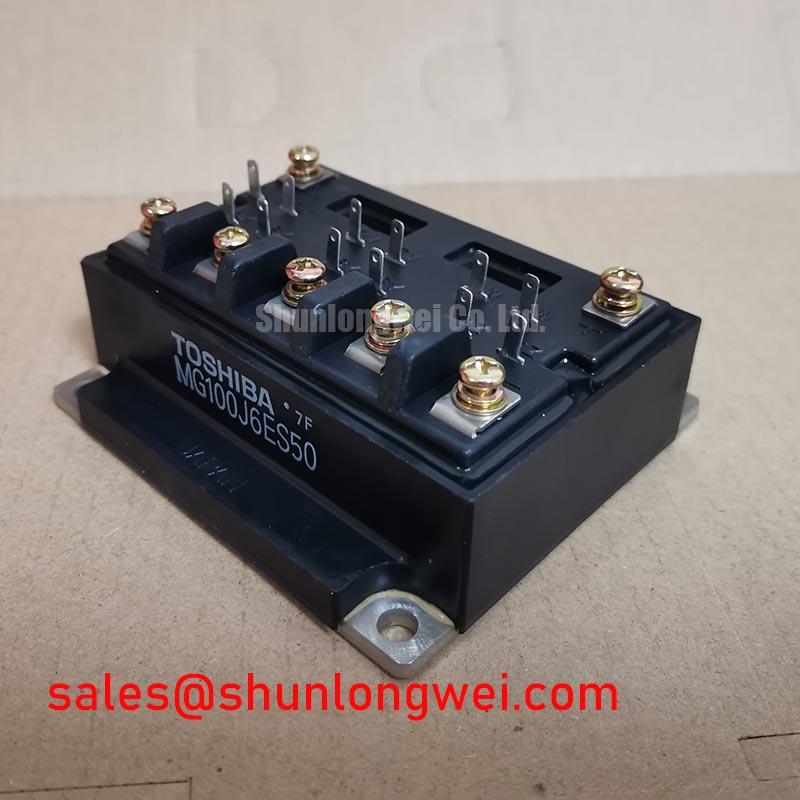
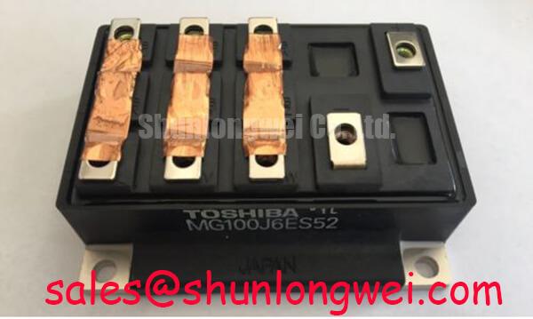
The Toshiba MG100J6ES52 is an IGBT Module with the following primary ratings: Collector-Emitter Voltage (Vces): 600.0 V and Rated Collector Current (Ic): 100.0 A under the manufacturer-specified conditions. Its product identification is Manufacturer: Toshiba, Part Number: MG100J6ES52, Package: Toshiba Module, and Configuration / Topology: IGBT Power Stage, with a three-phase inverter bridge configuration. Terminal assignments, rating test conditions, mounting limits, and insulation test conditions require the corresponding manufacturer datasheet.
For incoming inspection, keep the electrical record attached to the exact part number rather than grouping modules by appearance. The MG100J6ES52 product reference provides the model-specific procurement context; installation acceptance should also include the equipment’s mechanical drawing and gate-driver circuit.
Trace the isolation boundary between the control electronics and each floating gate-driver supply before investigating unexpected gate pulses. Design Consideration: common-mode transient immunity belongs to the driver and its surrounding circuit, not to the module’s collector-emitter voltage rating. A switching-node transition can disturb a driver through isolation capacitance, supply coupling, or an unsuitable return path without establishing that the power module itself is defective.
Compare the driver input command with the gate-emitter waveform using appropriately rated differential measurement equipment. Keep the measurement loop compact and reference the gate measurement to the corresponding emitter connection identified in the terminal drawing. An apparent narrow pulse should be checked for probe pickup before it is treated as genuine gate excitation. Record whether the disturbance follows the switching edge, a driver-supply dip, or an input-command transition.
Review terminal creepage and clearance against the assembled equipment’s working voltage, pollution environment, insulating materials, and applicable safety standard. These distances are properties of the complete assembly: adjacent busbars, mounting hardware, contamination, and wiring can change the effective insulation path. A reinforced-insulation classification or a withstand-test voltage must come from the relevant documented barrier, rather than being inferred from the 600.0 V semiconductor rating.
At the bench, use diode mode only after identifying the intended current path from the circuit diagram. Compare corresponding bridge positions with identical lead orientation and temperature, and separate external snubbers or driver connections where the service procedure permits. A diode-mode reading does not establish insulation withstand, switching recovery performance, or full-load health.
Bench Tip: Keep gate terminals under appropriate ESD control and compare cold-state readings only after confirming that the DC link is discharged.
If the equipment uses a bootstrap-powered driver, examine its supply waveform through the actual switching sequence. Recharge opportunities, diode behavior, and switching-node movement affect the available gate-drive supply; capacitor selection and acceptance limits belong to the driver design, not to an assumed MG100J6ES52 requirement.
MG100J6ES52 Thermal-Electrical Optimization: Optimizing Heatsink Contact Pressure and Practical Tuning
Inspect the heatsink mating surface for burrs, embedded debris, and uneven contact marks before reinstalling the module. Design Consideration: thermal-interface material should fill surface irregularities without becoming an unnecessarily thick thermal barrier. Select its application method and finished thickness from the interface-material instructions and the module mounting requirements, rather than assigning a universal coating thickness.
Check baseplate and heatsink flatness through the approved mechanical inspection method. Do not compensate for a visibly uneven mounting surface by increasing screw torque or adding an uncontrolled quantity of compound. Either approach can leave local gaps while changing package loading. Where the mounting instructions specify a staged or crossing sequence, follow that sequence with a calibrated torque tool and record the final setting.
Contact pressure depends on the actual fasteners, washers, mounting arrangement, and permitted package load. The Toshiba Module package designation alone does not establish bolt size or tightening torque. Keep power-terminal fastening requirements separate from baseplate mounting requirements, since they serve different mechanical functions.
During controlled recommissioning, observe temperature trends together with current, switching conditions, and coolant or airflow conditions. An external case-temperature measurement is not a direct junction-temperature measurement. A temperature imbalance warrants comparison of thermal contact, current loading of the bridge positions, and gate-drive waveforms before assigning a single cause.
For broader device-selection context, the IGBT versus MOSFET practical selection guide helps frame conduction and switching-loss tradeoffs. It does not replace the module-specific thermal characteristics needed to establish an operating envelope.
When evaluating an industrial inverter welder or medium-frequency induction-heating power supply, engineers should compare the required circuit arrangement, switching conditions, cooling interface, and terminal geometry with this module. A related part such as MG50Q6ES50 is a comparison candidate only; direct replacement requires a documented electrical, mechanical, and protection review.
MG100J6ES52 Circuit Protection & Reliability: Calibrating Diode Softness Factor and Switching Interaction
Capture commutation current and collector-emitter voltage together when investigating ringing around a diode-to-IGBT transition. Design Consideration: reverse recovery interacts with loop inductance and turn-on speed, so an abrupt current transition can contribute to overshoot and oscillation. Diode softness is a dynamic characteristic; a satisfactory cold-state forward reading cannot establish it.
Use consistent probe placement, operating temperature, and load conditions when comparing waveforms. Check measurement bandwidth and probe behavior before interpreting a sharp current feature as peak reverse-recovery current. The freewheeling path, external wiring, and adjacent switch operation all affect the observed transition.
Where measurements support a change, designers may evaluate turn-on gate damping or an RC snubber to reduce commutation stress. Gate resistance changes can alter switching loss and timing, while a snubber introduces its own dissipation and pulse-loading requirements. Component values should follow measured circuit behavior and the system’s validated limits, not a generic prescription attached to this part number.
Keep the high-current commutation loop compact to limit inductive overshoot, while preserving the assembly’s required insulation distances. Recheck gate and collector-emitter waveforms after layout or damping changes. Reduced ringing alone does not demonstrate acceptable device loss or system EMC compliance.
Finally, review protection coordination separately from normal switching behavior. Where regenerative energy handling is present, the braking chopper and resistor must be assessed against the equipment’s energy flow rather than inferred from the bridge current rating. Semiconductor fuse clearing behavior and protective shutdown timing likewise require coordination with documented device withstand characteristics. Acceptance should resolve measured voltage stress, protection response, and thermal loading under the equipment’s approved test procedure.