
Content last revised on September 10, 2026
Static and Dynamic Current Distribution across Paralleled IGBT Switches
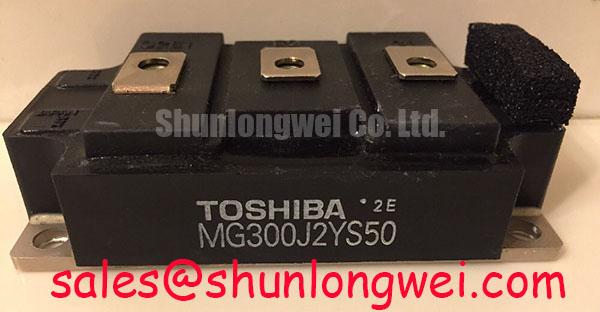
Operating heavy-duty variable frequency drives (VFDs) under punishing industrial duty cycles requires strict control over current balancing when configuring power stages. The Toshiba MG300J2YS50 is a dual-pack half-bridge module rated at VCES = 600V and continuous collector current IC = 300A (Official Datasheet Specification). When high-torque motor acceleration ramps or severe dynamic loads demand aggregate currents exceeding single-module capacity, engineering teams frequently deploy these modules in parallel configurations. Maintaining current parity across individual silicon dies under both static conduction and fast transient transitions determines whether a power conversion cabinet achieves decade-long reliability or suffers premature catastrophic switch failure.
Static current sharing relies primarily on the conduction characteristics of the internal power semiconductor dies. With an on-state saturation voltage rated at VCE(sat) = 2.7V at 25°C (Official Datasheet Specification), the forward voltage drop exhibits temperature-dependent behavior that design engineers must leverage. At higher junction temperatures, modern IGBT structures transition toward a positive temperature coefficient of saturation voltage. If one paralleled module carries a disproportionate share of the 300A nominal load, its silicon junction temperature increases, raising its internal conduction resistance and naturally diverting excess current into the cooler companion module. However, during light-load idling or lower junction operating states where the temperature coefficient may remain slightly negative or flat, static imbalances must be mitigated by matching terminal contact resistances, DC bus bar lengths, and phase output copper cross-sections to within strict engineering tolerances.
Dynamic current distribution presents far more severe operational hazards during microsecond-scale switching events. Turn-on and turn-off current sharing is heavily dictated by threshold voltage (VGE(th)) variations, internal gate resistance, and structural loop symmetry. If parasitic inductances in the gate drive or power loops differ by even a few nanohenries between paralleled branches, the module with the faster switching trajectory will momentarily absorb the entire rate of current change (di/dt), causing local junction overheating. Plant maintenance technicians diagnosing localized over-temperature warnings on paralleled inverter phases should check for identical gate harness lengths, symmetrical twisted pairs, and balanced DC-link connection geometries. For lower power sub-systems or auxiliary dynamic braking paths in the same cabinet architecture, smaller dual-pack configurations such as the MG50G2DM1 provide a compatible structural topology for scaled drive sections.
Routine plant floor troubleshooting should incorporate regular verification of dynamic current sharing using calibrated flexible Rogowski coils or clip-on high-bandwidth DC current probes on each collector branch during full-load motor acceleration runs. Any phase leg displaying a static current divergence exceeding 10% between paralleled paths signals developing terminal oxidation, uneven thermal paste degradation, or mismatched gate drive output impedance that requires immediate mechanical retorquing and driver circuit inspection.
Planar Symmetrical Busbar Geometry: Achieving L_sigma < 20nH to Protect Silicon Junctions
In high-capacity AC motor drive systems, minimizing DC-bus parasitic stray inductance (Lσ) is essential to preserve the 600V collector-emitter breakdown rating of the MG300J2YS50. During hard turn-off transitions under heavy motor overload, the high rate of current change across the collector terminals generates a severe transient overvoltage spike across the silicon switch. The peak voltage seen by the internal IGBT equals the DC-link operating voltage plus the product of total stray loop inductance and the turn-off di/dt rate. Without rigorous busbar inductance suppression, this inductive flyback voltage can easily breach the absolute maximum voltage threshold, puncturing the reverse-blocking junction layer.
To restrict total loop inductance (Lσ) to below 20nH, modern industrial inverter design dictates the implementation of laminated planar busbars rather than point-to-point discrete cable harnesses. Planar busbars superimpose wide, thin copper conduction plates separated by high-dielectric insulating films (such as Kapton, Nomex, or polyester sheets) in close physical proximity. The magnetic flux produced by forward current traveling through the positive DC plate is effectively canceled by the equal and opposite return current traversing the adjacent negative plate. This mutual electromagnetic flux cancellation suppresses loop inductance down to negligible industrial baselines, keeping peak transient spikes safely within the continuous 600V silicon boundary even during emergency fault interruptions.
High-frequency film snubber capacitors must be integrated directly across the DC positive and negative input terminals of the module. Installing low-ESR, low-inductance polypropylene snubber capacitors within 15 to 25 millimeters of the terminal connections creates a localized high-frequency AC loop that absorbs inductive energy before it reaches the main silicon dies. On the AC mains supply side, coordinated metal oxide varistor (MOV) surge absorption networks are implemented alongside bidirectional transient voltage suppressors across the DC link. These protective elements ensure that upstream utility surges, inductive kickbacks from long motor cables, or regenerative energy bursts from dynamic braking cycles do not stress the power semiconductor baseplates.
💡 Pro Tip: During scheduled preventive maintenance cycles, always inspect the mechanical clamping torque on laminated busbar terminal interfaces. Loose hardware increases contact resistance, distorts the balanced current path between parallel dielectric layers, and degrades the low-inductance coupling geometry. Apply an insulated torque wrench to maintain factory-specified mechanical tolerances across all terminal lugs, ensuring that vibration from surrounding industrial machinery does not introduce localized parasitic inductance pockets.
Optimizing Gate Drive Loop Geometry to Prevent Cross-Conduction Oscillation
The internal configuration of the Toshiba MG300J2YS50 features dual half-bridge switches that require robust, high-integrity gate drive isolation to prevent shoot-through failures. A primary root cause of catastrophic phase-leg short circuits in heavy-duty variable frequency drives is spurious gate turn-on caused by common-mode ground bounce and high dv/dt Miller current injection. When the complementary switch transitions rapidly, the inter-electrode collector-to-gate capacitance (Miller capacitance) forces displacement current into the inactive gate loop. If the gate drive return path shares common impedance with the high-current power emitter circuit, the resulting inductive voltage drop lifts the local gate voltage above the conduction threshold, triggering momentary phase shoot-through.
To eliminate mutual emitter coupling, the control circuitry must utilize dedicated auxiliary Kelvin emitter terminals that isolate the low-power gate drive return current from the 300A main emitter power track. Routing the gate command and auxiliary emitter return as a tightly twisted pair or as stripline traces on inner printed circuit board layers minimizes the physical loop area, substantially reducing susceptibility to ambient electromagnetic interference emitted by neighboring power stages.
Implementing an active negative gate bias during the off-state (typically applying a gate turn-off voltage between -5V and -8V) provides critical noise margin against spurious turn-on. Even if high transient dv/dt induces transient displacement current across the Miller capacitance, the negative bias holds the gate well below the turn-on threshold, ensuring reliable blocking. In addition, localized gate damping resistors must be sized to damp high-frequency LC tank circuits formed by the module input capacitance and parasitic lead inductances without excessively slowing down the switching speed. When conducting root-cause failure analysis on inverter boards following catastrophic silicon rupture, field technicians can consult the diagnostic testing and fault analysis workflows documented in the Field Engineer’s Handbook to distinguish between gate-loop oscillations and pure thermal runaway signatures.
Diagnostic verification on the factory floor requires connecting high-bandwidth, electrically isolated differential oscilloscope probes directly across the gate and auxiliary emitter pins under full-load motor acceleration. Technicians must inspect the waveform for parasitic high-frequency ringing, ground-bounce spikes exceeding the safety threshold, or slow voltage tails that indicate failing driver output stages or compromised optical isolator couplers.
Evaluating Thermal Capacitance vs Heat Sink Time Constant under Surge Bursts
Thermal management in heavy-duty industrial drives requires balancing short-term silicon thermal capacitance against long-term heatsink dissipation time constants. The Toshiba MG300J2YS50 features an absolute maximum junction temperature rating of Tj = 150°C and an electrical isolation capability of Viso = 2500V AC for one minute (Official Datasheet Specifications). During severe motor stall conditions, hard conveyor start-ups, or bidirectional regenerative braking bursts, the silicon junction experiences immense instantaneous power dissipation peaks that drive junction temperatures toward their structural limit long before the bulk aluminum heatsink shows any perceptible temperature rise.
The transient thermal impedance (Zth(j-c)) of the internal copper baseplate and direct bonded copper (DBC) ceramic substrate governs the initial milliseconds of a thermal overload. The silicon die possesses a minute thermal capacitance, allowing its junction temperature to surge within 10 to 50 milliseconds during an overcurrent event. Conversely, large forced-air or liquid-cooled aluminum heatsinks exhibit thermal time constants ranging from 60 seconds to over 10 minutes. Engineers must calculate thermal safety margins using multi-RC Foster or Cauer thermal equivalent networks to verify that transient peak junction temperatures never exceed 150°C during worst-case peak surge current (ITSM) events, allowing adequate cool-down recovery intervals between duty cycles.
| Parameter / Mechanical Metric | Official Rating / Engineering Value | Operational Role in Motor Drives |
|---|---|---|
| Collector-Emitter Voltage (VCES) | 600 V | DC bus voltage ceiling with transient overshoot headroom |
| Continuous Collector Current (IC) | 300 A | Continuous phase current capability at nominal baseplate temperature |
| Saturation Voltage (VCE(sat)) | 2.7 V (Typical at 25°C) | Determines steady-state conduction loss and thermal dissipation |
| Max Junction Temperature (Tj) | 150 °C | Upper thermal limit for silicon integrity during transient bursts |
| Isolation Voltage (Viso) | 2500 V AC (1 min) | Galvanic safety barrier between internal circuit and chassis baseplate |
| Mounting Bolt Torque (M5 Baseplate) | 2.5 – 3.5 N·m | Industry standard torque to prevent thermal interface voiding |
Preventive maintenance teams must focus on preserving the thermal interface material (TIM) layer between the module baseplate and the cooling assembly. Over thousands of operational hours in high-vibration, high-thermal-cycling environments, thermal grease is subject to degradation, pump-out, and dry-out. This results in microscopic air pockets, sharply increasing the case-to-heatsink thermal resistance (Rth(c-s)). Facility maintenance schedules should mandate periodic thermal imaging scans calibrated against radiometric thermal measurement guidelines established by organizations like the National Institute of Standards and Technology (NIST) to identify phase-to-phase temperature deltas exceeding 8°C under identical load conditions.
⚠️ Maintenance Note: When overhauling variable frequency drives during planned plant shutdowns, clean all heatsink cooling fins of industrial dust, oil residue, and conductive particulate buildup. When reinstalling or replacing an IGBT module, thoroughly remove old silicone grease with an appropriate solvent, apply a uniform 50 to 100-micron layer of high-stability synthetic thermal compound using a screen-printing stencil, and tighten all baseplate mounting bolts in a two-step diagonal cross pattern to 2.5–3.5 N·m. Uneven mounting torque warps the internal ceramic substrate, resulting in localized hot spots and dielectric fracture under high thermal cycling stress.