Content last revised on September 10, 2026
BSM400GA120DN2S_E3256 Specifications and Evaluation Overview
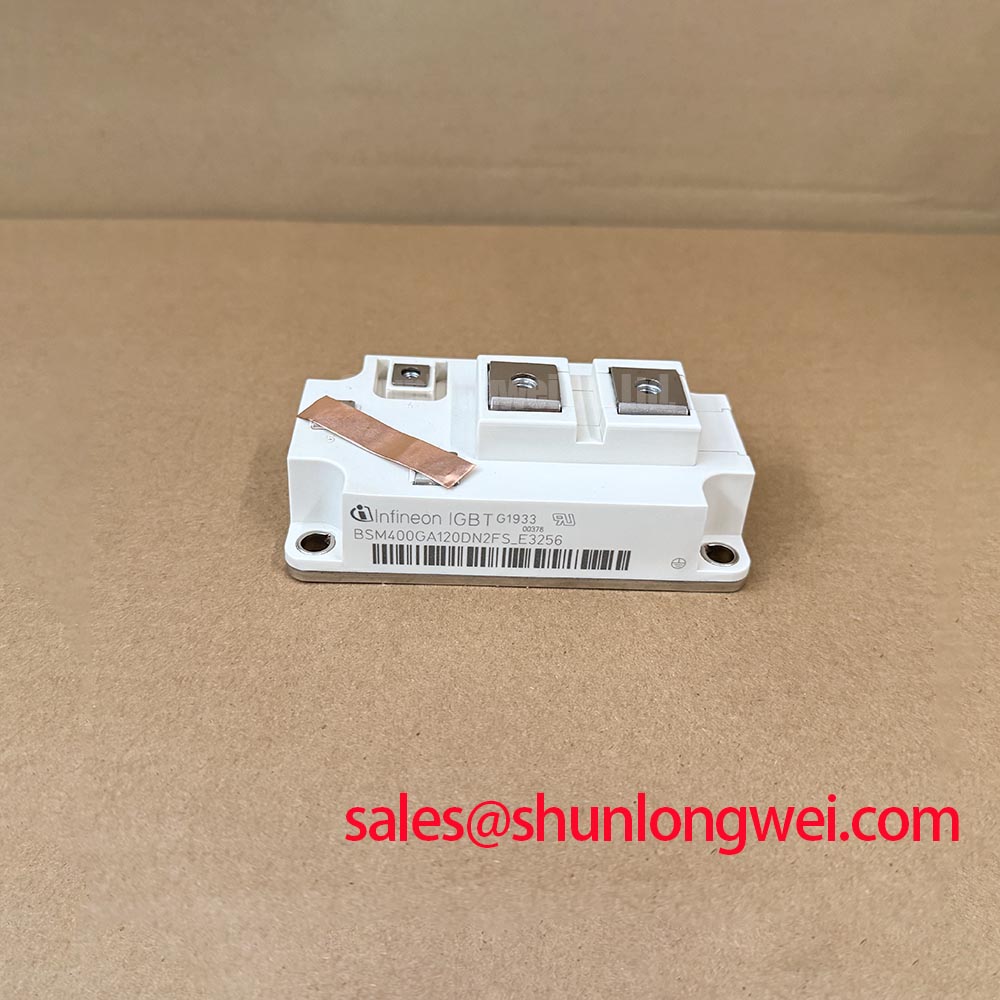
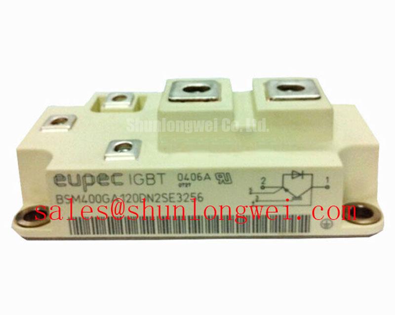
Begin a service evaluation by isolating the power stage, inspecting the module body and terminals, and verifying the original equipment rating before applying any test voltage. The BSM400GA120DN2S_E3256 is an Infineon single switch standard power module specified at 1200 V collector emitter voltage and listed with a 400 A collector current rating. Its listed typical saturation voltage is 2.50 V, while the maximum junction to case thermal resistance is 0.06 K/W. The gate emitter peak voltage rating is ±20 V.
These figures are official product specifications supplied for this device. They define electrical boundaries for evaluation, but they do not by themselves establish a complete converter operating point, short circuit withstand time, switching speed, insulation system, EMC compliance, or field lifetime. Engineers assessing the module for a utility scale centralized battery energy storage power conversion system should match the part against the original switching cell, gate driver arrangement, cooling path, bus structure, protection sequence, and operating duty.
| Technical specification | Value |
|---|---|
| Manufacturer | Infineon |
| Product type | Single switch standard power module |
| Collector emitter voltage, VCES | 1200 V |
| Collector current rating, IC | 400 A |
| Gate emitter peak voltage, VGES | ±20 V |
| Saturation voltage, VCE(sat) | 2.50 V typical |
| Junction to case thermal resistance, RthJC | 0.06 K/W maximum |
BSM400GA120DN2S_E3256 Circuit Protection & Reliability: Calibrating Desaturation Detection
The device rating should be verified against the actual DC link and switching transient envelope before the replacement module is energized. A 1200 V VCES rating is an official specification, not permission to operate at an assumed bus voltage without measuring turn off overshoot. Stray inductance in the commutation path can raise collector emitter voltage during a fault or normal switching transition, so the protection study should use oscilloscope measurements taken at the module terminals with a suitable high voltage differential probe.
Desaturation protection is implemented by the external gate driver and its sensing network unless the equipment documentation states otherwise. The driver monitors the collector emitter condition after the turn on sequence and initiates a controlled response if the expected low voltage state is not reached. This helps distinguish a hard short circuit, a failed gate drive path, excessive current, or abnormal commutation from a routine switching event. The exact blanking interval, fault threshold, filtering, and response time must be selected from the driver documentation and verified with the module and converter topology. A requirement such as detection within a particular number of microseconds cannot be assigned to this module without an authoritative short circuit test specification.
For type I and type II short circuit studies, the test engineer should record gate voltage, collector current, collector emitter voltage, driver supply behavior, and fault propagation at the same time base. The short circuit safe operating area and permitted fault duration must come from the applicable Infineon documentation for this exact device and test condition. If that data is unavailable, the safe approach is to treat the duration as system determined rather than infer it from the 400 A collector current rating. Continuous current and short circuit withstand are different electrical conditions.
A two stage soft turn off is an engineering recommendation for review where a direct gate discharge would create excessive inductive voltage. The first stage can reduce the current transition rate, while the second stage completes turn off after the driver has confirmed the fault response. The actual gate resistance, timing, clamp level, and protection coordination require double pulse and controlled fault testing. The objective is to limit collector emitter overshoot while still removing channel conduction quickly enough to protect the semiconductor.
Gate loop layout deserves the same attention as the desaturation threshold. Keep the outbound and return paths close together, separate high current commutation copper from the gate control route, and avoid sharing a noisy emitter return with the driver reference unless the module documentation explicitly defines a suitable auxiliary terminal. This part is identified as a single switch module in the supplied specification, so any Kelvin emitter connection must be confirmed from the original mechanical and electrical drawing rather than assumed from general IGBT practice.
During field troubleshooting, compare the suspect phase with a known good phase under the same low energy test condition. Check whether the desaturation signal changes when the gate driver is disabled, whether the fault occurs at turn on or during commutation, and whether the driver supply dips at the event. An unexpected fault indication may involve probe placement, gate loop oscillation, diode recovery in the wider circuit, a damaged driver, or a genuine power stage fault. The waveform sequence should be verified before replacing additional components.
Preventing Spurious Faults: High-Altitude Cosmic-Ray-Induced SEB Failure Guidelines for BSM400GA120DN2S_E3256
High altitude operation introduces a reliability question that cannot be answered from the published voltage, current, saturation voltage, and thermal resistance values alone. Terrestrial neutron exposure can influence single event effects in power semiconductors, but a credible single event burnout assessment requires device specific test data, the actual DC link voltage, switching state, shielding environment, altitude profile, mission duration, and an accepted reliability model. No FIT rate, burnout probability, or altitude derating factor should be presented for this module without an Infineon qualification report or a recognized standards based source.
The practical engineering response is to review the DC link headroom under worst case regeneration, battery fault conditions, control overshoot, and elevated installation altitude. The design team should obtain the applicable Infineon ruggedness information and use it with the converter reliability process. A conservative voltage derating may be evaluated as a design consideration, but its numerical value must be determined by the system owner from validated device data rather than copied from an unrelated IGBT family.
Gate power integrity also needs attention when the switching cell uses a floating high side driver. A bootstrap arrangement is topology dependent and is not an inherent feature of this single switch module. The capacitor selection should account for total gate charge over the intended voltage swing, driver quiescent consumption, leakage, temperature, refresh interval, switching frequency, and permissible driver supply ripple. The system integrator should verify that the capacitor remains adequately charged during the longest high side conduction interval and during fault handling. If the converter uses an isolated gate supply, the isolation supply design and its transient behavior should be assessed instead.
To investigate nuisance protection events, measure the driver supply directly at the driver pins while recording the gate emitter waveform and the desaturation line. A supply dip, excessive common mode displacement, or a poorly referenced sensing return can produce a fault report without proving that the IGBT has failed. The diagnostic sequence should include a gate resistance check, driver output symmetry, isolation barrier behavior, and the physical routing of the collector voltage sense path.
The Infineon IGBT Modules Overview provides broader manufacturer context for module selection and application evaluation. It should not be treated as a substitute for the exact technical documentation applicable to the BSM400GA120DN2S_E3256. The same distinction applies when comparing a discrete power module with an intelligent module family such as the Infineon CIPOS™ Intelligent Power Modules, since integrated sensing and protection features vary by product family.
Transient Dynamics & Electrical Design: High dv/dt Cross Conduction Shoot Through on BSM400GA120DN2S_E3256
In a bidirectional battery energy storage PCS, the module may be evaluated alongside other switches in a bridge or phase leg. High dv/dt at one switch can couple through device capacitances and the physical gate loop of another switch. The resulting gate disturbance can reduce the intended dead time margin and create cross conduction. This is a system level switching interaction, not a failure mode that can be diagnosed from VCE(sat) alone.
An active Miller clamp may be considered when the selected driver supports it and when the measured common mode transient produces a problematic gate excursion. The clamp should connect to the driver reference using a low impedance path and should be evaluated with the actual module layout, isolation barrier, gate resistor network, and switching frequency. A negative gate bias can also be considered for turn off, but the permitted gate emitter range remains bounded by the official ±20 V VGES rating. The selected bias value must come from the driver and system design after testing; a fixed negative voltage should not be assumed for this module.
Gate loop parasitic inductance can create ringing when the driver current changes rapidly. Minimize the loop area, keep the gate resistor physically close to the gate connection, and prevent the power commutation path from running parallel to sensitive gate traces. Damping should be tuned from measured gate emitter and collector emitter waveforms rather than selected from a generic value. Excessive resistance can slow switching and increase loss, while insufficient damping can increase ringing and false turn on risk.
High voltage clearance and creepage must be checked around the module terminals, bus bars, driver isolation interface, and any conductive mounting hardware. The required distances are determined by working voltage, pollution degree, material group, altitude correction, insulation type, and the applicable equipment standard. The module voltage rating does not certify the complete assembly insulation system. Designers should document the spacing calculation and inspect for contamination, loose hardware, solder debris, and damaged insulation after service work.
When a bridge reports intermittent shoot through, use a controlled low energy switching test and capture both gate signals at the power module. Verify the actual dead time at the pins, not only the controller command. Compare the turn off tail, gate rebound, driver common reference movement, and opposite switch gate response. If the observed fault changes with probe grounding or cable position, measurement coupling may be involved. Recheck the signal path with differential or isolated instrumentation before changing protection thresholds.
Pro Tip: Keep the gate drive return physically separate from high current emitter or source current paths, then confirm the resulting common mode behavior with switching waveforms rather than continuity measurements alone.
For service planning, the BSM75GD120DLC can be reviewed as a related Infineon device, but electrical, mechanical, thermal, and gate drive compatibility must be established from its own documentation before any substitution decision. It should not be treated as an automatic replacement for the BSM400GA120DN2S_E3256.
Assembly Integrity & Layout Architecture: Evaluating Thermal Capacitance vs Heat Sink for BSM400GA120DN2S_E3256
The supplied maximum junction to case thermal resistance of 0.06 K/W is a steady state thermal specification for the specified reference path. It does not describe the complete transient response of a battery PCS power stage. Short overloads, repetitive current pulses, switching loss, contact resistance, thermal interface condition, baseplate temperature, and heatsink thermal capacitance all influence junction temperature. A multi element RC thermal model may be used as an engineering calculation, but its parameters must be sourced from the applicable manufacturer thermal data or validated through testing.
For a pulsed overload evaluation, begin with measured collector current and switching voltage waveforms. Estimate conduction and switching losses using the actual gate drive, junction temperature, load power factor, commutation device behavior, and switching conditions. Feed the resulting loss profile into the selected transient thermal model, then compare the calculated junction temperature with the official maximum rating from the exact device documentation. If the transient model is not validated, use it to identify sensitivity to pulse width and cooling changes rather than to claim a guaranteed peak junction temperature.
Mechanical assembly has a direct effect on the thermal path. The mounting surface should be clean, flat, and free from burrs. The thermal interface material should be applied consistently according to its manufacturer instructions, with no voids or excessive thickness created by uneven clamping. Fastener sequence and torque must follow the Infineon mechanical documentation for this package and the hardware used. A generic torque value is not an official parameter for this particular module.
Inspect the bus bar interface for uneven contact, discoloration, loosened fasteners, and signs of local heating. A high current module can show normal electrical continuity while still suffering from poor pressure distribution or elevated interface resistance. Thermal imaging under a controlled load can locate phase imbalance, but the camera reading should be correlated with thermocouples or other suitable sensors because surface emissivity and access conditions affect the result.
The module should be placed so that the high current loop is compact and symmetrical with respect to the intended commutation path. This reduces parasitic inductive voltage during switching and helps the gate driver operate against a more predictable reference. The control board, isolation components, and power terminals should be mechanically supported so that vibration or service access does not load the module terminals. The final arrangement should be checked against the enclosure insulation, cooling airflow, bus bar temperature, and applicable creepage requirements.
In the rectifier and front end portion of a converter, engineers may also review the related BSM75GB120DN2 as an associated device reference. Its ratings and topology are separate from those of the BSM400GA120DN2S_E3256, so the rectifier stage must be analyzed independently for current sharing, reverse recovery interaction, thermal loading, and protection timing.
Commissioning should proceed from low energy gate checks to reduced bus voltage, then to controlled load steps while monitoring collector emitter voltage, gate emitter voltage, case temperature, driver supply, and fault lines. The engineering record should retain the measured waveforms, thermal interface details, mounting inspection results, and protection response. For broader integration guidance covering gate drive, thermal management, and circuit topology, consult IGBT Design & Integration.