Content last revised on September 19, 2026
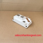
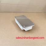
BSM400GA120DN2FS-E3256 Specifications and Replacement Inspection
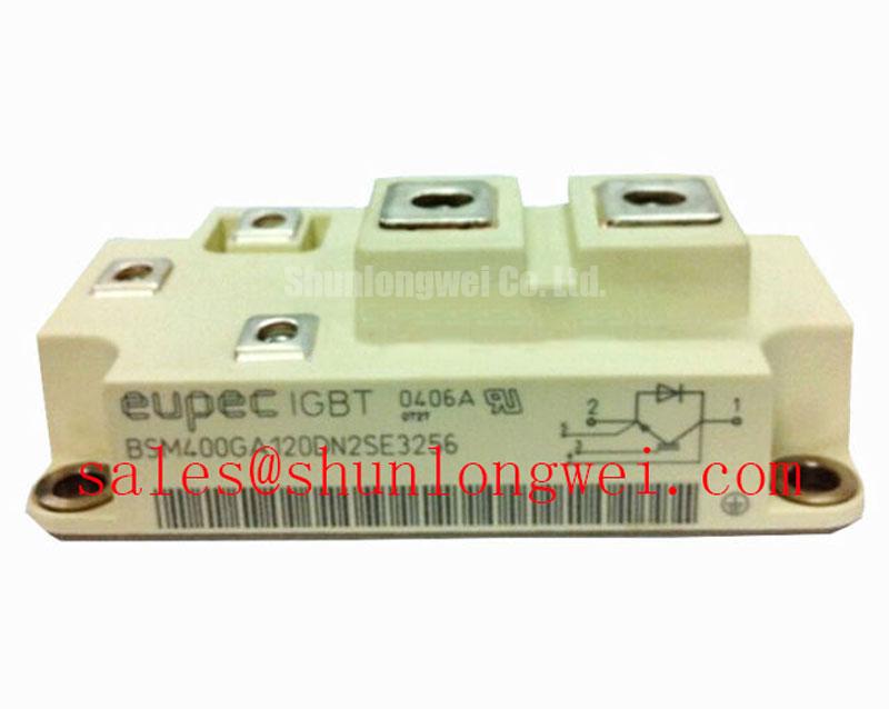
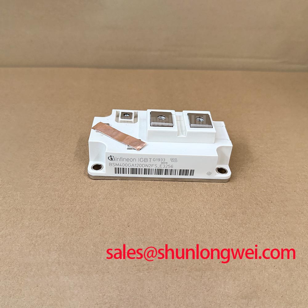
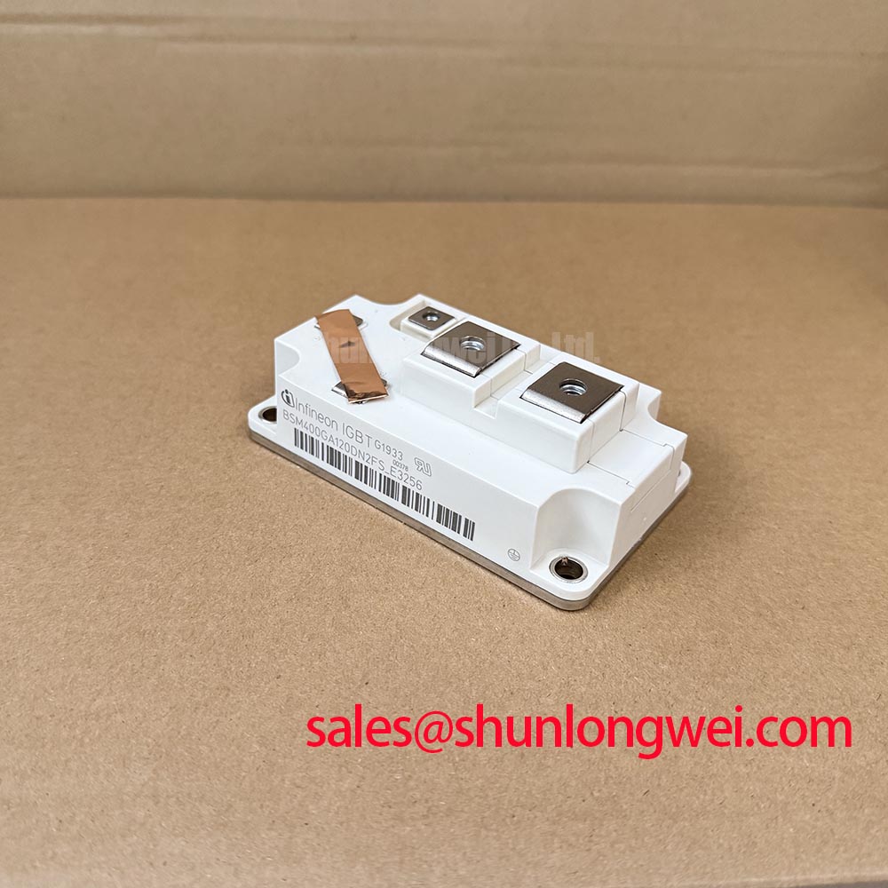
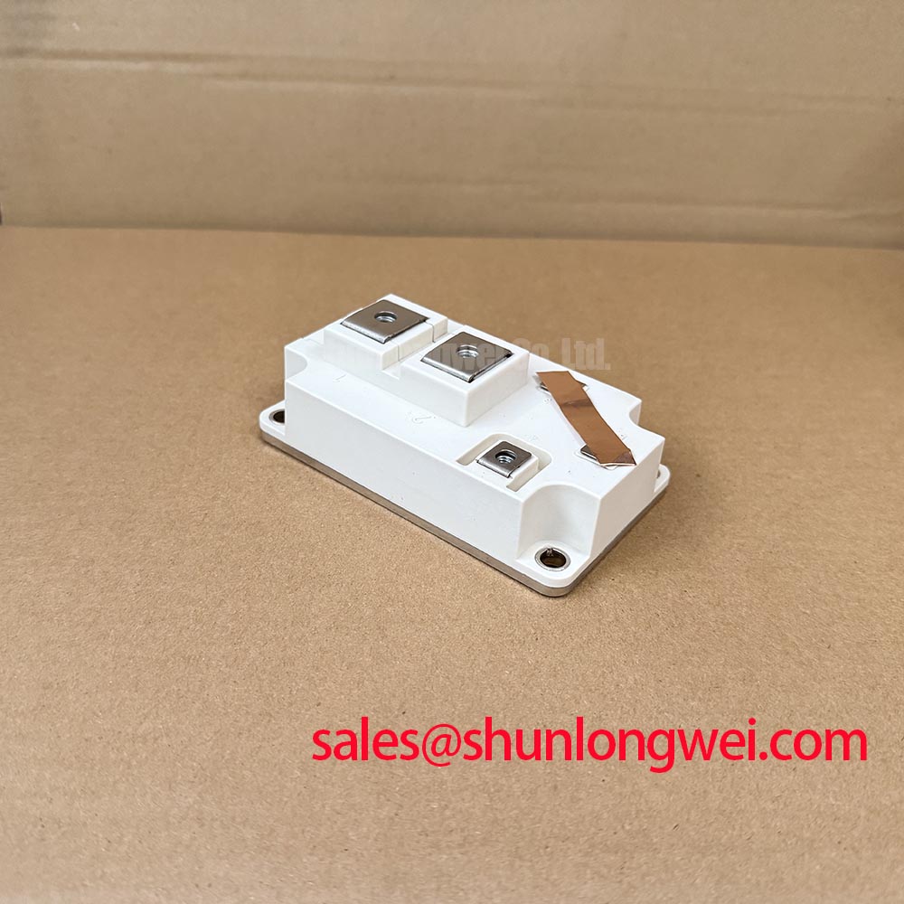
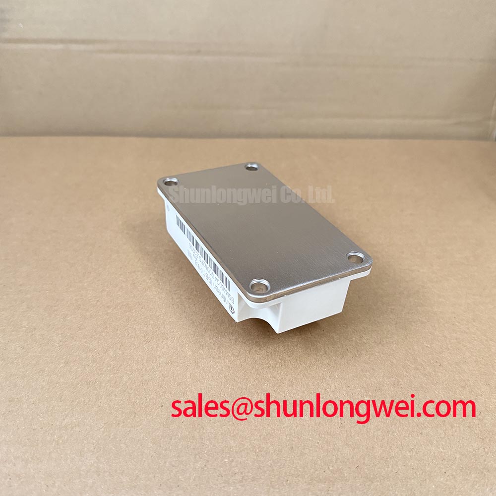
Before fitting the BSM400GA120DN2FS-E3256, isolate the converter, inspect the power terminals and housing for mechanical damage, then compare the installed module marking and DC bus rating against the service documentation. This Infineon IGBT module is officially rated at VCES = 1200 V, with continuous DC collector current of 400 A at TC = 80°C and 550 A at TC = 25°C. Those values establish the electrical identity that must match the original inverter leg or power conversion assembly before any replacement work proceeds.
The module has an official typical collector emitter saturation voltage of VCE(sat) = 2.5 V at Tj = 125°C, a maximum chip to case thermal resistance of RthJC ≤ 0.045 K/W, and a pulsed collector current capability of 1100 A at TC = 125°C. Its insulation test rating is 2500 Vac for 1 minute. These figures are Official Datasheet Specifications and should be checked against the equipment’s original power stage documentation, cooling interface, gate driver board, and DC link arrangement.
| Official specification | Value | Service relevance |
|---|---|---|
| Collector emitter voltage, VCES | 1200 V | Defines the module’s stated blocking voltage boundary. |
| Continuous DC collector current, IC | 400 A at TC = 80°C | Relevant to sustained converter loading with the intended case temperature. |
| Continuous DC collector current, IC | 550 A at TC = 25°C | Represents the stated current condition at a lower case temperature. |
| Collector emitter saturation voltage, VCE(sat) | 2.5 V typical at Tj = 125°C | Supports conduction loss assessment under the stated test condition. |
| Thermal resistance, RthJC | ≤ 0.045 K/W maximum | Describes the chip to case thermal path. |
| Pulsed collector current, ICpuls | 1100 A at TC = 125°C | Must not be treated as a continuous operating current rating. |
| Insulation test voltage, Vis | 2500 Vac for 1 minute | Official dielectric test specification for the module insulation system. |
BSM400GA120DN2FS-E3256 Circuit Protection & Reliability: High Altitude and Cosmic Ray Evaluation
For a utility scale centralized battery energy storage PCS installed at elevated altitude, the first practical task is to establish the actual DC bus waveform, including switching overshoot, regeneration events, and transient behavior during grid disturbances. The 1200 V VCES value is an Official Datasheet Specification, not a guarantee that every external transient or layout induced voltage spike remains within that boundary. Field measurements should therefore be taken at the module power terminals with a correctly rated differential measurement method and compared with the system’s validated voltage limits.
Terrestrial neutron exposure and single event burnout are high risk reliability subjects. No device specific FIT rate, altitude derating curve, cosmic ray failure probability, or service life figure is stated in the supplied official specifications for this module. It would therefore be inappropriate to calculate a numerical SEB rate or prescribe a fixed DC bus derating value. As a Design Consideration, equipment teams operating above approximately 2000 m should review site altitude, enclosure cooling conditions, installed surge protection, switching waveform records, and the manufacturer’s system qualification requirements before approving the operating envelope.
A metal oxide varistor network, surge clamp arrangement, and DC link capacitor bank must be assessed as parts of the converter assembly rather than as properties of the IGBT module. Their role is to limit externally generated surge energy and reduce the likelihood that cable inductance or busbar inductance creates a terminal voltage excursion during switching. The system engineer should verify clamp coordination against the measured DC bus transient, the module’s 1200 V blocking rating, and the actual energy conditions of the PCS.
At the service bench, check the heatsink contact plane, terminal hardware, busbar flatness, and evidence of insulation contamination before energizing a repaired cabinet. Clearance and creepage distances are determined by the complete assembly, including conductor geometry, pollution environment, insulation material, and applicable equipment standards. The module’s 2500 Vac for 1 minute insulation test rating must not be interpreted as confirmation that the surrounding busbar system, driver board, enclosure, or wiring harness meets a particular insulation coordination standard.
⚠️ Field Alert: Disconnect and verify discharge of the DC link before removing gate or power connections, because retained energy and accidental gate drive can damage the replacement module and surrounding assembly.
If a damaged inverter leg is being evaluated for a same family comparison, BSM75GD120DLC can be reviewed as a separate module reference, but its current capability, package arrangement, gate drive requirements, thermal interface, and circuit topology must be confirmed from the original equipment documentation. It should not be assumed to be a direct substitute for the BSM400GA120DN2FS-E3256.
Benchtop Waveform Tuning: Mitigating Stress via Bi Directional DC DC Buck Boost Conversion on BSM400GA120DN2FS-E3256
In a bidirectional battery energy storage PCS, power can move from battery racks to the inverter DC link and back toward the battery system. During commissioning, observe both directions of power flow because reverse energy transfer can expose a gate drive or busbar issue that is absent during one directional operation. The BSM400GA120DN2FS-E3256 should be evaluated as part of the complete switching cell, including the complementary device path, DC link capacitors, gate driver isolation, current sensing, and controller interlock logic.
Dead time is system determined. It must be sufficient to prevent cross conduction during commutation while avoiding an unnecessary increase in diode related loss and thermal cycling. An Engineering Recommendation is to validate the chosen timing with switching waveforms measured under the actual battery voltage, current direction, temperature, and load transition conditions. A controller setting that appears acceptable at low power may require reassessment during high current peak shaving events.
Gate loop routing deserves close attention when replacing a module or reconnecting a driver board. Keep the gate and emitter return path compact to reduce parasitic loop inductance, particularly where fast current change can create gate voltage disturbance. If the package and original driver board provide a dedicated auxiliary emitter or sensing return connection, the system integrator should identify its intended routing from the equipment documentation rather than assuming terminal functions from physical location alone. Separating the driver return from the high current power path can help reduce common mode ground bounce when the original circuit design supports it.
A negative gate turn off bias is a Design Consideration used in some IGBT driver implementations to improve immunity to unintended turn on. Whether it is appropriate, and the required value, depends on the official driver specification, gate voltage limits, isolation architecture, and measured switching behavior. Do not introduce a negative bias supply solely because it is present in another converter design. Confirm gate emitter voltage directly during turn off and inspect for ringing, delayed gate discharge, or coupling from the opposite switch node.
Where the PCS has a distinct auxiliary or rectifier related stage, BSM75GB120DN2 is a relevant component reference for topology review. Its presence in another stage does not establish electrical interchangeability with this 1200 V, 400 A module. Compare voltage rating, current rating, package, control interface, cooling path, and equipment bill of materials before selecting any service replacement.
Benchtop Waveform Tuning: Mitigating Stress via Multi Module Parallel Current Sharing on BSM400GA120DN2FS-E3256
When several power modules are operated in parallel, current balance must be demonstrated in the assembled converter. The typical 2.5 V VCE(sat) value at the stated junction temperature is useful for understanding conduction behavior, but it is not a standalone promise of equal current sharing between modules. Differences in cable resistance, busbar geometry, heatsink temperature, gate timing, device variation, and measurement reference can alter both steady state and transient current distribution.
For static sharing, modules should experience closely matched thermal and power connection conditions. For dynamic sharing, use a symmetric gate drive layout wherever the converter architecture permits it. The critical aim is to avoid one module receiving an earlier or stronger gate command due to unequal routing impedance. The appropriate damping network, gate resistor selection, and driver output capability are system determined and should be verified using captured gate emitter voltage and collector emitter voltage waveforms.
A useful maintenance sequence begins with an unpowered inspection. Confirm that parallel power paths have equivalent mechanical seating, that busbar joints are clean and flat, and that gate connectors are fully engaged. After controlled energization, compare phase current signals and thermal observations across the parallel positions. A persistent imbalance may indicate unequal driver behavior, a connection issue, sensor offset, cooling variation, or a control loop problem. It should be investigated with waveform evidence rather than attributed to one cause without testing.
The 1100 A pulsed collector current value is an Official Datasheet Specification at TC = 125°C; it does not authorize arbitrary repetitive surge operation in a parallel arrangement. Peak current capability depends on the complete pulse duration, junction temperature, switching conditions, protection response, and converter duty cycle. The equipment design authority should validate current sharing during the intended transient events and confirm that protection reacts correctly when one parallel path becomes abnormal.
For broader context on switching technologies and their design tradeoffs, see Wide Bandgap Revolution. That technical discussion can help frame a platform level review, while the service decision for this module must remain based on the original IGBT converter design and the official specifications of the BSM400GA120DN2FS-E3256.
Assembly Integrity & Layout Architecture: Optocoupler and Digital Coreless Transformer Gate Drive Review
Before reconnecting the gate driver, identify whether the original converter uses an optocoupler based isolation path or a digital isolator architecture such as a coreless transformer solution. These approaches have different propagation behavior, supply arrangements, fault handling, and common mode characteristics. The driver board should be retained or replaced according to the original equipment design; neither approach can be declared superior for this module without the system’s switching frequency, isolation requirement, controller design, and validation results.
The supplied module specification confirms 2500 Vac for 1 minute insulation test capability. It does not specify reinforced isolation above 5 kV, common mode transient immunity above 100 kV/µs, or independent system EMC compliance. Those requirements belong to the driver, printed circuit board, mechanical clearances, cable system, enclosure, and end equipment standard. Designers should verify isolation ratings and common mode transient immunity from the actual gate driver documentation, then test the assembled power stage under representative switching conditions.
During an emergency repair, inspect gate drive supply rails, desaturation or overcurrent protection wiring, fault return paths, and controller inhibit signals before applying high voltage. A spurious gate pulse can result from poor return routing, connector damage, inadequate isolation behavior, control sequencing, or measurement interference. Probe the gate emitter signal against the intended local reference and compare it with a known good phase where available. This provides a more reliable diagnosis than judging the driver from a static continuity test alone.
Use the module’s stated maximum RthJC of 0.045 K/W when reviewing the thermal chain, while remembering that the heatsink, interface material, mounting pressure, fan performance, coolant condition, and cabinet airflow remain external system factors. Apply thermal interface material uniformly according to the equipment maintenance procedure and verify that the module sits flat against the heatsink. A thermal issue can elevate switching and conduction stress even when static semiconductor checks appear normal.
For manufacturer level context on power semiconductor portfolios and integration approaches, consult Infineon High Power Semiconductor Solutions and Infineon CIPOS™ Maxi IPM Series. These references describe broader product families; they do not replace verification of the original PCS schematic, driver board documentation, and module specific operating limits.