
Content last revised on November 11, 2026
1MBI400NA-120-02 Initial Electrical Checks
With the DC link isolated and verified discharged, disconnect the gate driver before checking collector-to-emitter and gate-to-emitter resistance on the 1MBI400NA-120-02. Record the meter polarity and compare readings with an electrically isolated, known-good position using the same instrument settings. Connected snubbers, driver components, and parallel power paths can influence readings; a cold resistance check is an initial screening step, not proof of switching performance.
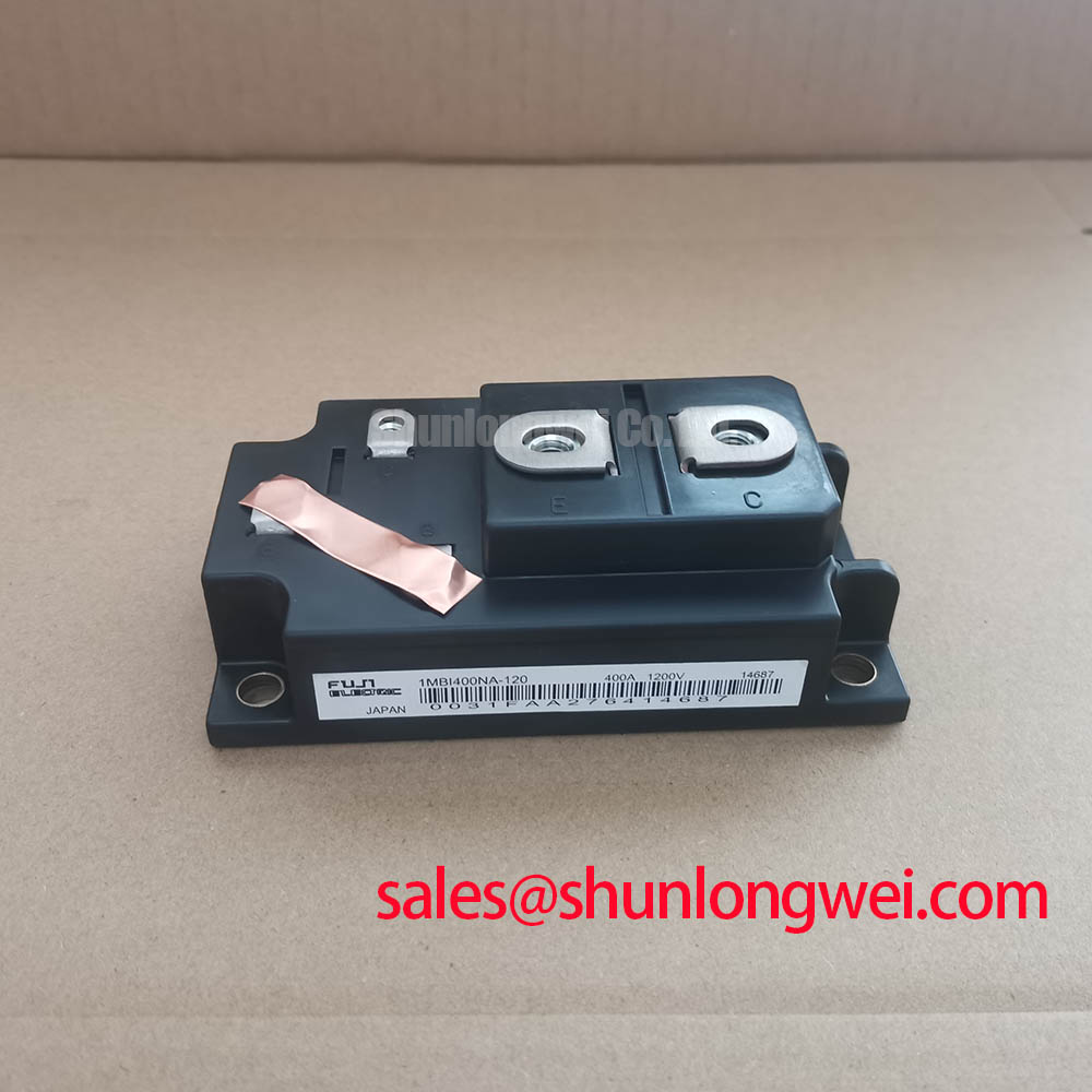
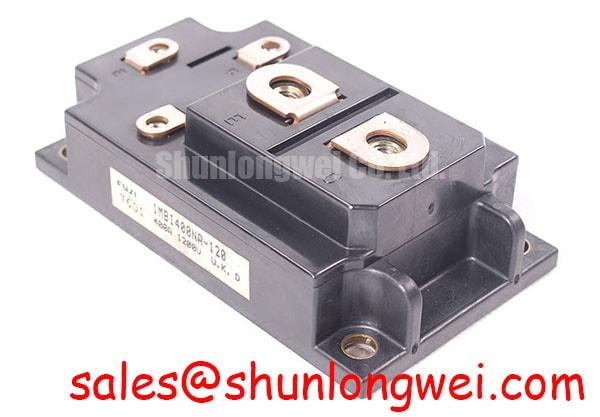
The primary ratings are Collector-Emitter Voltage (Vces): 1200.0 V and Continuous Collector Current (Ic): 400.0 A under the specified conditions (Official Specification). Product identification is Manufacturer: Fuji Electric; Part Number: 1MBI400NA-120-02; Package: Fuji Power Module; and Configuration / Topology: IGBT Power Stage, with a single-switch configuration. For replacement assessment, consult the model-specific datasheet for terminal assignments, rating conditions, gate limits, switching characteristics, and mounting requirements.
Assembly Integrity & Layout Architecture: Implementing Derating Guidelines and Mismatched Parameters for 1MBI400NA-120-02
Compare the parallel branches before disturbing the busbar assembly: unequal conductor lengths, displaced gate wiring, and uneven cooling interfaces can make otherwise similar switching positions behave differently. Design Consideration: static current sharing depends on the devices’ on-state characteristics at the actual operating current and temperature. A positive collector-emitter saturation-voltage temperature coefficient can assist sharing where the relevant characteristic curves demonstrate that behavior; it should not be assumed across the entire operating range for this module.
Dynamic balance needs separate attention. Match the electrical geometry of corresponding gate-drive paths, including their return conductors, rather than judging symmetry from cable length alone. Different loop areas and shared return impedance can produce unequal switching transitions even when steady-state current appears balanced. During controlled testing, compare branch current and gate-emitter waveforms under equivalent load conditions, keeping probe placement consistent.
Design Consideration: a laminated DC-link busbar can reduce commutation-loop inductance when outgoing and returning current paths remain closely coupled. Inspect whether replacement hardware introduces separated conductors, extended terminal adapters, or displaced capacitor connections. These changes can increase turn-off overshoot. Determine acceptable geometry from measured switching stress and the equipment’s electrical clearances, rather than applying an unsupported universal inductance target.
When assessing a utility-scale centralized battery energy storage PCS, evaluate this single-switch module against the actual converter schematic, cooling arrangement, and bidirectional operating sequence. Battery charging and discharging can impose different current and thermal histories. Engineering Recommendation: examine temperature excursions during representative transitions and adjust operating limits through the system’s validated thermal model, without assigning an unsupported service-life extension.
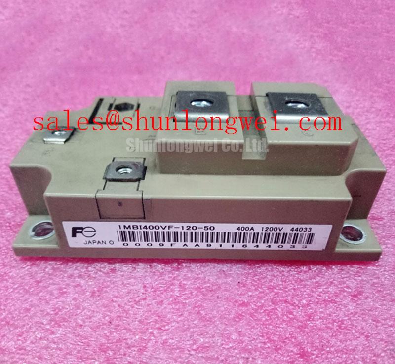
The 1MBI400HH-120-50 provides a related model for comparison, not an automatic substitute. Check terminal geometry, gate-drive requirements, switching behavior, and thermal characteristics before considering interchangeability. Matching headline voltage and current ratings alone does not establish a drop-in replacement.
Assembly Integrity & Layout Architecture: Implementing Auxiliary Emitter Pinout Cold-Check for 1MBI400NA-120-02
Trace the driver return from the equipment schematic to the module terminal drawing before assigning any small terminal as an auxiliary emitter. A continuity measurement can establish an electrical connection, but cannot establish the intended current path or prove an internal Kelvin connection. Keep terminal identification tied to the exact module drawing and equipment wiring record.
Design Consideration: where the documented terminal arrangement provides a dedicated auxiliary emitter return, route the gate-driver return through that connection rather than through a load-current conductor. Voltage developed across shared emitter-path inductance during current transitions changes the effective gate-emitter voltage. This can distort switching timing or contribute to unintended gate excitation. The objective is to reduce shared impedance, not to claim that any routing arrangement eliminates ground bounce.
For the cold check, isolate the driver harness and compare its conductor mapping with the schematic. Inspect connector seating, conductor damage near strain reliefs, and any repair that joins the signal return to a power terminal elsewhere in the assembly. An apparently convenient return connection can bypass the intended driver-loop architecture. Avoid probing an unidentified terminal with an energized driver.
Thermal assessment belongs alongside this wiring inspection because switching frequency affects the heat that the cooling assembly must remove. Engineering Recommendation: evaluate the equipment’s intended frequency range using switching-loss information at relevant current, voltage, gate resistance, and temperature conditions. Do not extrapolate one operating point into a module-wide derating curve.
Check fan direction, obstructed heat-exchanger passages, interface seating, and temperature-sensor placement before increasing load. Higher inlet-air temperature or reduced airflow can change the usable operating envelope even when the driver wiring is correct. Keep module case measurements distinct from terminal temperatures and inferred junction temperature; they describe different parts of the thermal path.
Benchtop Waveform Tuning: Mitigating Stress via Main Power Terminal Contact Resistance on 1MBI400NA-120-02
Measure each accessible power-terminal joint with a four-wire micro-ohmmeter after isolating parallel measurement paths. Place the voltage-sense contacts so the reading represents the intended interface rather than an uncontrolled length of busbar. Record probe locations and joint temperature; otherwise, comparisons made before and after reassembly can be misleading.
Design Consideration: assess contact resistance against the equipment’s approved assembly criteria and comparable sound joints, not an invented module-specific acceptance threshold. Increased resistance produces localized heating under load, but a low cold reading does not demonstrate adequate contact pressure throughout thermal cycling. Inspect mating surfaces, fastener condition, washers, and mechanical support for conductors that could load the terminal sideways.
Field Alert: Keep the assembly de-energized during terminal work, and use the documented fastening sequence, tightening torque, and thermal-interface procedure rather than a generic bolt-size rule.
Under an authorized, controlled load test, compare thermal images of equivalent terminal positions at similar current and cooling conditions. Account for surface emissivity and reflections before interpreting an apparent hot spot. A temperature difference should prompt examination of the joint, conductor loading, and cooling exposure; it does not identify one cause by itself.
Once the connections are mechanically sound, inspect collector-emitter overshoot and ringing with appropriately rated differential measurement equipment. Engineering Recommendation: keep the measurement loop compact and distinguish probe-induced ringing from the circuit response before changing gate resistance or snubber components. The Snubber Loss Balancing Technical Reference provides context for evaluating transient suppression alongside the extra dissipation introduced by a snubber.
Keep resistance measurements, thermal images, and waveform captures associated with the exact 1MBI400NA-120-02 product identification in the maintenance record. This helps procurement and service teams compare the requested part with the installed assembly without treating neighboring model numbers as equivalent.
1MBI400NA-120-02 Operational Boundaries: Evaluating Negative Gate Bias vs Active Miller Clamp Limits
Observe the off-state gate-emitter waveform while the complementary switching position commutates, using the documented emitter reference and a probe arrangement suitable for the common-mode transient. Design Consideration: collector-gate capacitance couples displacement current into the gate circuit during rapid collector-voltage transitions. The resulting gate excursion depends on the driver’s sink capability, gate-path impedance, return inductance, and the operating point.
Reverse-transfer capacitance, often identified as Cres, and gate-charge information describe related but different aspects of this behavior. Neither provides a universal clamp setting by itself. Evaluate the complete switching transition rather than treating a single capacitance value as constant throughout the voltage swing.
A negative off-state bias and an active Miller clamp address the gate disturbance differently. Engineering Recommendation: select any negative bias within the module’s documented gate-emitter limits and the driver’s operating boundaries. For an active clamp, examine its engagement timing, sink-current capability, and physical return path. A clamp placed behind a long, inductive connection cannot be assessed from its driver datasheet alone.
Adjust replacement gate resistance only through controlled testing that compares turn-on behavior, turn-off overshoot, gate ringing, and driver dissipation. Slower switching can reduce some transient stresses while increasing switching loss; the appropriate balance belongs to the equipment’s operating conditions. Fuji Electric’s RC-IGBT modules overview offers context on a separate product family, not evidence that its architecture or gate requirements apply to this model.
Before restoring normal operation, verify that the measured off-state gate excursion, switching peaks, and protection response remain within the approved equipment limits across representative load transitions. Retain those captures with the driver settings so subsequent service work can distinguish an assembly change from a change in operating conditions.