

Content last revised on September 10, 2026
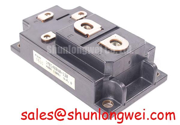
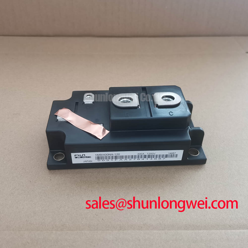
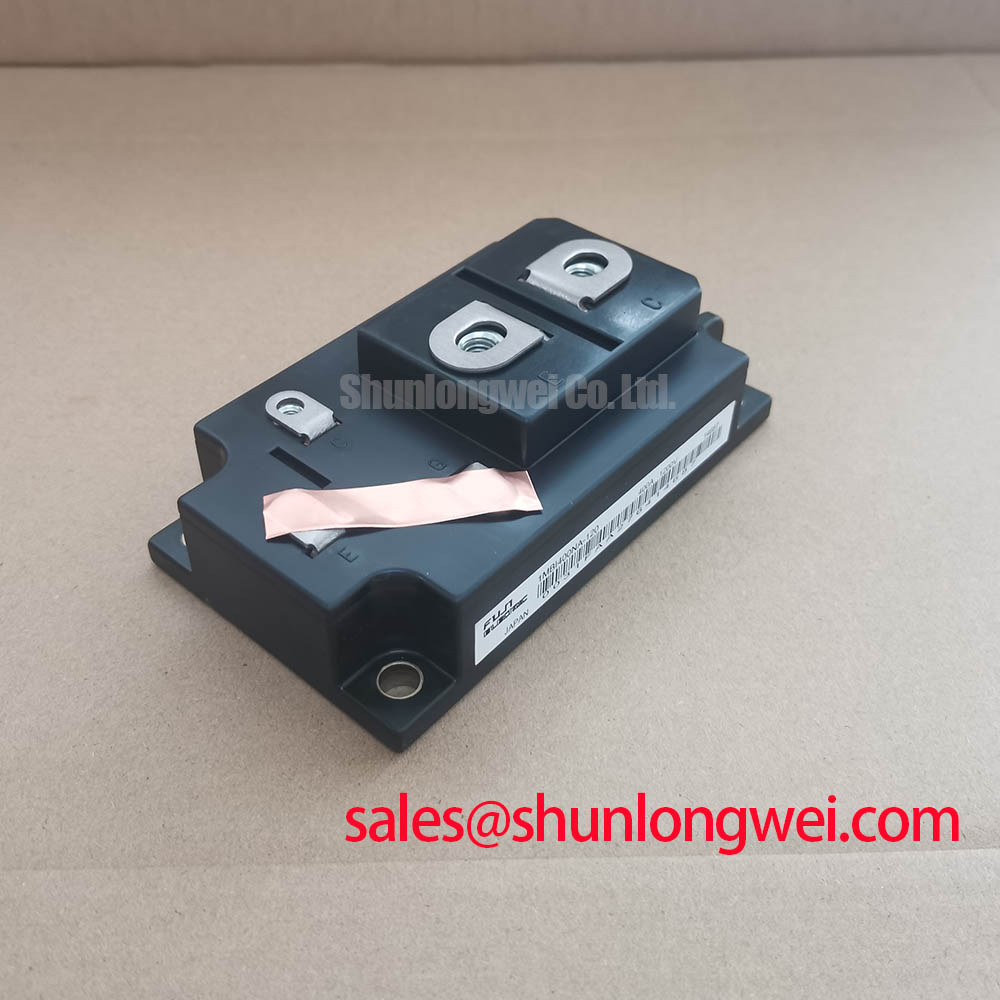
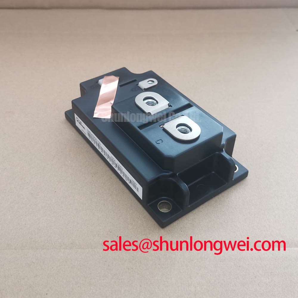
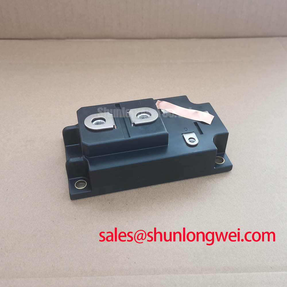
1MBI400NA-120 Fuji Electric 1200V 400A IGBT Module
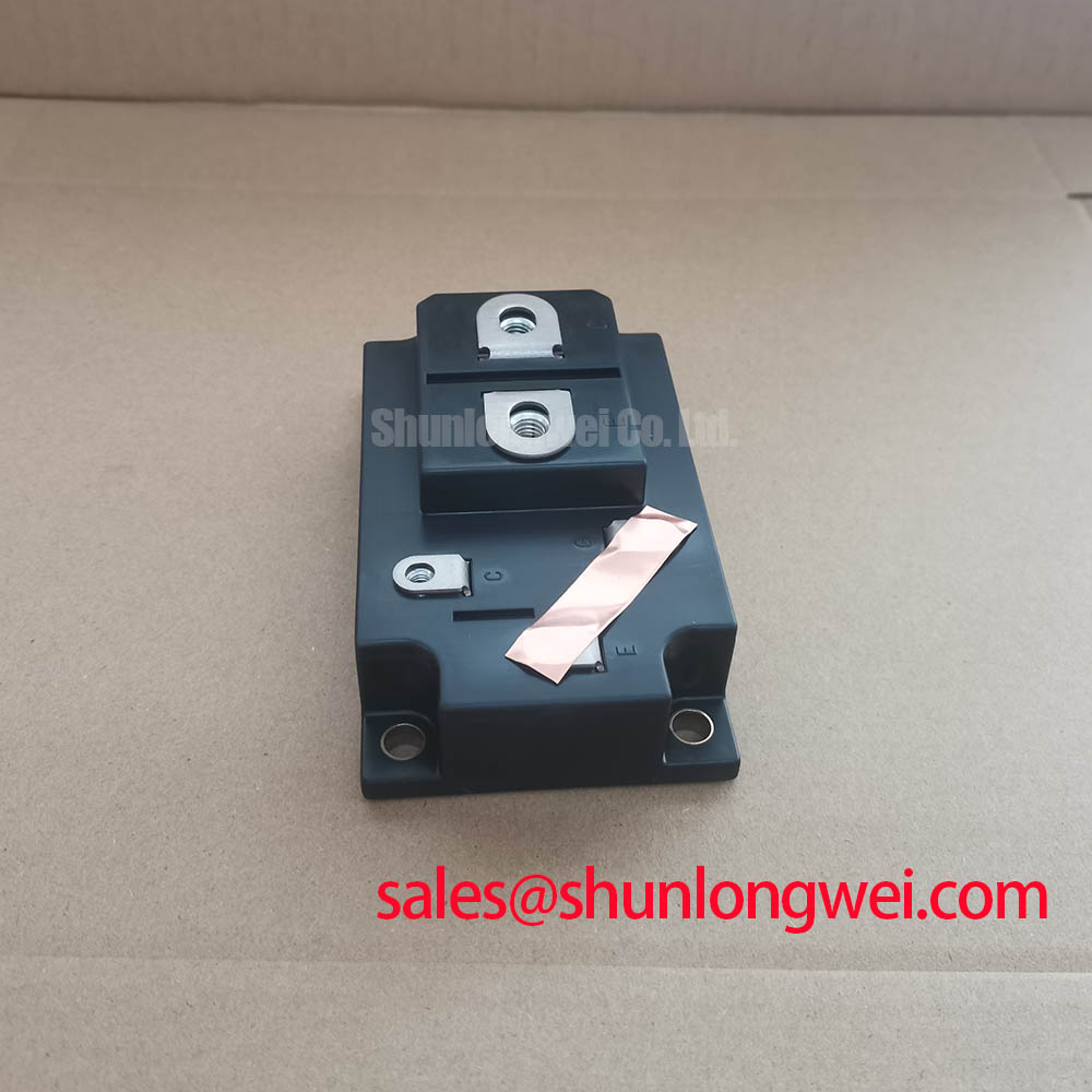
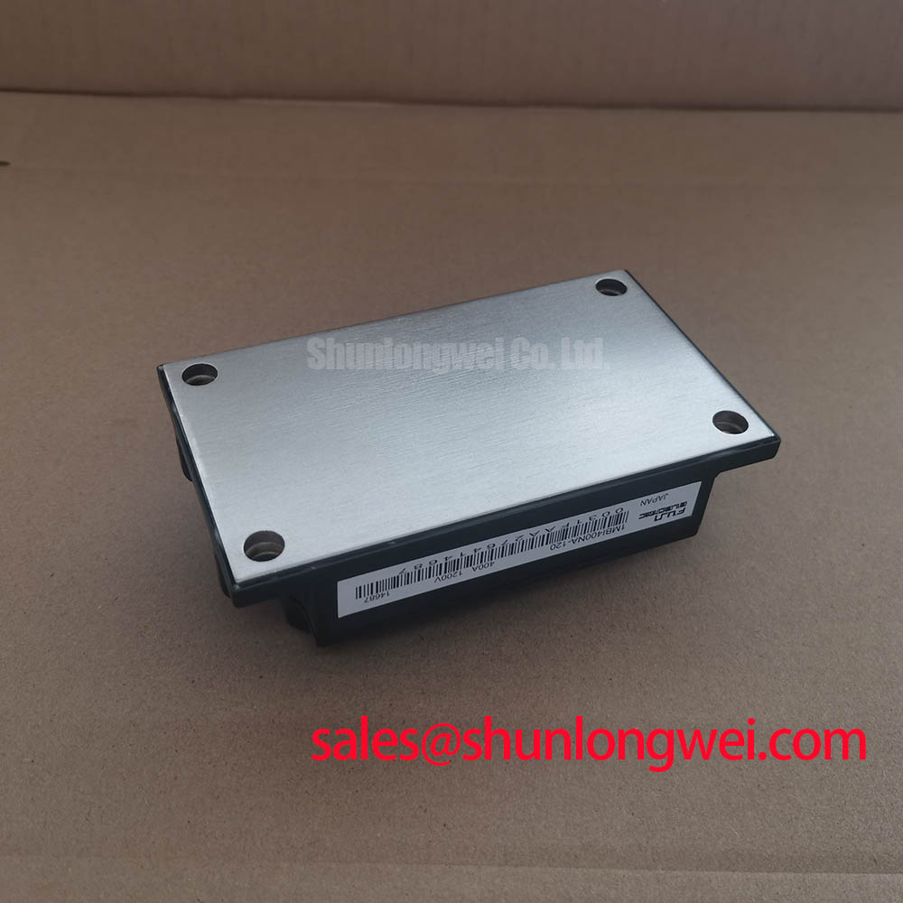
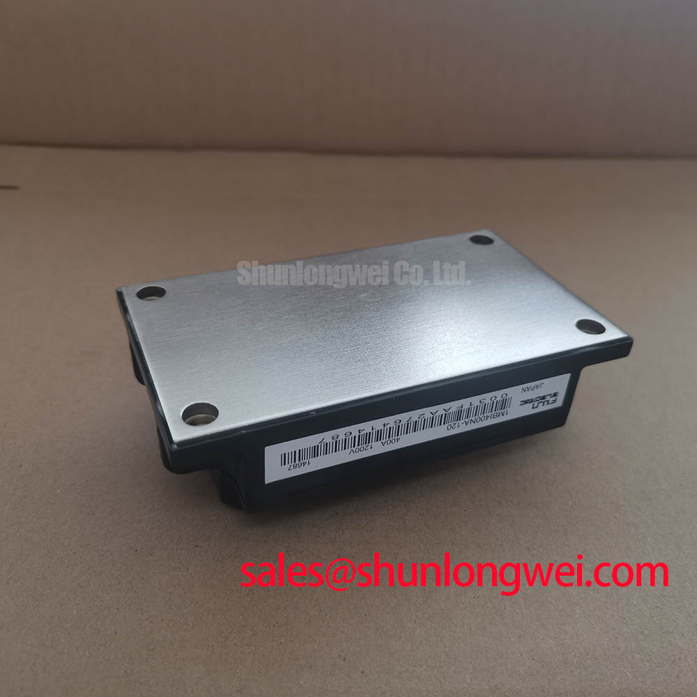
Before energizing a replacement, inspect the module body and terminals, confirm the marking against the equipment record, and verify the manufacturer data: 1MBI400NA-120 is a Fuji Electric IGBT Module specified at 1200 V and 400.0 A, with a Module package classification.
For maintenance teams working on high power conversion equipment, these three values establish the initial identity and electrical boundary of the part. They do not replace a complete design review. The installed circuit, switching frequency, cooling system, gate driver, protection timing, and DC link conditions must all be checked against the original equipment documentation before commissioning.
| Specification | Value | Classification |
|---|---|---|
| Manufacturer | Fuji Electric | Official product identification |
| Model | 1MBI400NA-120 | Official product identification |
| Rated voltage | 1200 V | Official Specification |
| Rated current | 400.0 A | Official Specification |
| Package | Module | Official Specification |
Assembly Integrity and Layout Architecture for 1MBI400NA-120
In a bidirectional battery energy storage PCS, the power stage alternates between charging and discharging. That four quadrant operating pattern means the IGBT module can experience repeated changes in current direction and switching duty. The practical maintenance priority is to keep the electrical path, mechanical clamping, and thermal interface stable as the equipment moves through peak shaving, charge recovery, and standby operation.
During inspection, check the busbar contact surfaces for discoloration, localized heating, loosened fasteners, and signs of uneven pressure. A laminated busbar arrangement can reduce commutation loop area, but its actual performance depends on the complete assembly, including terminal geometry, insulation spacing, capacitor placement, and the current return path. Designers should minimize parasitic loop inductance to control turn off overshoot, then verify the measured collector emitter waveform during switching tests rather than relying only on a layout estimate.
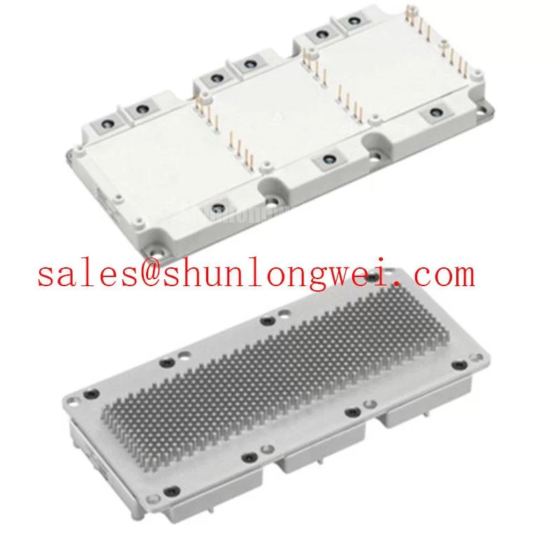
The module base and heatsink interface also require controlled preparation. Remove degraded thermal compound, clean both mating surfaces with a suitable process, and inspect for scratches, distortion, or contamination. A thin and continuous thermal interface layer is generally preferred as a Design Consideration, while the correct compound type, application method, clamping sequence, and fastening torque must follow the applicable Fuji Electric documentation and the equipment builder’s assembly procedure.
Double sided cooling arrangements require particular attention to parallelism and pressure distribution. A flat mounting surface and an even cross tightening sequence help prevent one side of the module from carrying excessive mechanical load. Where spring washers or disc springs are used, maintenance personnel should verify their condition, installed orientation, and compression calibration against the original assembly drawing. Substituting a different spring stack without confirming the mechanical load path can alter both thermal contact and module stress.
The gate drive wiring should remain physically separated from high current commutation paths wherever the equipment layout permits. Keep the gate return path short and direct, and inspect connectors for oxidation, loose crimping, or damaged locking features. A suspected switching fault should be compared with a known good phase using an oscilloscope and appropriate isolation practices. Static resistance checks alone cannot confirm correct gate timing or dynamic immunity.
For a compatible replacement assessment, engineers may also review the neutral product information for 2MBI400TB-060-01. It should not be treated as an automatic substitute. Terminal arrangement, electrical ratings, gate characteristics, mechanical dimensions, protection coordination, and thermal performance must be verified at system level.
Maintenance Note: Monitor contact temperature trends during scheduled service and clear accumulated dust from the heatsink and airflow path before thermal alarms become intermittent.
Preventing Spurious Faults from Atmospheric Neutron Effects
Atmospheric radiation effects, including terrestrial neutron exposure, are reliability topics for high voltage power semiconductor systems, particularly where installation altitude, switching stress, and DC link conditions differ from the original qualification environment. A field service page should not assign a FIT rate, claim a Single Event Burnout probability, or prescribe an altitude derating value without an authoritative device reliability study and the relevant system data.
For the 1MBI400NA-120, the appropriate Design Consideration is to verify the applied voltage and transient peak at the module terminals under the worst credible operating state. This includes battery rack voltage variation, regeneration, control faults, emergency shutdown, unequal phase current, and the interaction between the module and its snubber network. Voltage headroom must be established from the verified official rating and the complete switching waveform, not from nominal bus voltage alone.
In the hardware inspection process, examine the laminated busbar joints, capacitor connections, and module terminals as one commutation system. An apparently tight connection can still produce excessive transient energy if the current path is physically long or the return plane is poorly coupled. Film snubber capacitors should be located according to the actual switching loop and validated with probing methods that do not add misleading lead inductance. The engineer should confirm the peak collector emitter voltage and ringing frequency under representative current conditions.
Where a PCS operates above two thousand metres, altitude related cooling and insulation considerations should be reviewed as part of the enclosure and power stage assessment. The module itself should not be presented as independently certified for a particular altitude or radiation environment unless the manufacturer provides that qualification. Designers should obtain the original application limits and use system testing to establish appropriate operating margins.
Fuji Electric’s technical information on Brake Chopper IGBT Modules can provide useful context for protection and switching behavior. It does not replace the specific data required for this model, its driver, or the complete battery converter. Related application principles are also discussed in the Industrial Applications resource.
Suppressing Cres Induced Gate Voltage Spikes
Fast collector voltage transitions can couple through the device’s reverse transfer capacitance and associated parasitic paths into the gate circuit. In a half bridge or bidirectional PCS leg, that coupling may appear as an unwanted gate voltage movement on the opposite device. The result can be false turn on, increased switching loss, abnormal current overlap, or a protection trip that appears only at a particular load condition.
The correct response is to inspect the complete driver loop. Measure the gate emitter waveform at the module terminals using a low inductance probing arrangement, then compare it with the driver output and the corresponding collector emitter transition. The measurement should be repeated during both charging and discharging power flow because the commutation path changes with current direction.
An active Miller clamp can be considered where the gate driver architecture supports it. Its suitability depends on driver isolation, propagation delay, gate loop impedance, common emitter behavior, and the switching sequence used by the PCS controller. Negative gate bias may also be evaluated by the system designer, but the required value must come from the driver design, the module’s approved operating information, and measured switching behavior. It should never be assumed from a generic IGBT application.
Gate resistance is another system tuning variable rather than a fixed product instruction. A higher resistance can slow the voltage transition and reduce ringing in some layouts, while excessive resistance can increase switching loss and affect short circuit protection timing. Engineers should tune the driver using measured gate voltage, collector emitter voltage, current overlap, and fault response, with the final setting determined by the complete power stage.
When an unexplained desaturation trip occurs, inspect the gate connector, isolated power supply, driver reference, current feedback, and probe setup before attributing the fault to the module. Compare the signal path with a healthy phase under the same operating command. This approach helps separate a genuine overcurrent event from a driver timing issue, common mode disturbance, or measurement artifact.
Transient Thermal Protection and Reliability Calibration
In a utility scale centralized battery energy storage PCS, the thermal condition of an IGBT module is governed by conduction loss, switching loss, cooling resistance, coolant or airflow stability, and the duration of each power pulse. A short peak shaving event and a sustained charge cycle can produce different junction temperature responses even when their average current readings appear similar.
Thermal verification should begin with the actual heatsink or cold plate condition. Check fan operation, filter loading, airflow direction, coolant circulation where applicable, and sensor placement. Inspect the thermal interface after abnormal temperature rise, especially if the module has been removed and reinstalled. Pump out, dry areas, contamination, or uneven clamping can increase thermal resistance without creating an immediately visible electrical fault.
A multi RC thermal model may be used as an Engineering Calculation to estimate the junction response from measured power pulses and the applicable junction to case data. The model must use the manufacturer’s published thermal information for the relevant module and should be checked against measured case temperature, electrical loss estimates, and protection records. Because the official parameters supplied for this product identify voltage, current, and package classification only, no additional transient thermal impedance or junction temperature limit should be invented for the product page.
Short circuit protection deserves a separate commissioning check. The desaturation circuit should detect the intended collector emitter condition, apply the approved soft shutdown sequence, and coordinate with the gate driver’s fault latch and controller response. Verification should be performed at the actual gate drive supply, temperature range, load condition, and wiring configuration used in the PCS. A soft shutdown that is acceptable at low current may not provide the same voltage stress control during a high energy fault.
Engineers should also review the physical spacing around the module, snubber, busbar, and gate driver. Clean insulation surfaces, secure barriers, and controlled cable routing reduce the chance that contamination, condensation, or common mode coupling will complicate fault diagnosis. For equipment exposed to low temperatures followed by rapid enclosure heating, anti condensation measures and cabinet environmental control should be evaluated by the system integrator.
Fuji Electric’s information on 7th Gen X Series IGBT Modules offers broader manufacturer context for IGBT technology, while the specific operating limits for 1MBI400NA-120 must remain tied to its applicable documentation. Before returning a PCS to service, record the terminal condition, cooling inspection, gate waveform, switching overshoot, protection response, and thermal trend so future maintenance has a reliable comparison point.