Content last revised on October 9, 2026
Preventing Spurious Faults: FIT and SEB Considerations for FF400R12KE3_B2
| Manufacturer | Infineon |
| Model | FF400R12KE3_B2 |
| Product Category | IGBT Module |
| Rated Voltage | 1200.0 V |
| Rated Current | 400.0 A |
| Package | Module |
Begin field evaluation by recording the DC bus voltage, switching state, installation altitude, and cooling condition before attributing a fault to the FF400R12KE3_B2. This Infineon module is specified at 1200.0 V and 400.0 A; those are official device ratings, while the usable operating point in a utility-scale battery energy storage PCS is determined by the converter topology, switching transient, thermal path, protection response, and operating environment.
Single Event Burnout and terrestrial neutron effects require a qualified reliability model, device-specific test data, and a defined mission profile. A precise FIT value cannot be inferred from the voltage rating alone. At installations above approximately 2000 m, atmospheric radiation exposure and cooling performance can both change, so the reliability review should combine altitude, DC bus history, junction-temperature estimates, switching duty, and protection records. Treat any calculated SEB or FIT figure as an Engineering Calculation only when its radiation model, device data, and statistical confidence are documented.
A practical design consideration is to preserve electrical headroom between the highest measured switching voltage and the module’s rated blocking voltage. The engineering team should capture turn-off overshoot at the power terminals under the intended battery charge and discharge profiles, then compare the measured peak with the applicable protection boundary. Minimize the commutation loop area and keep the high-current path mechanically stable; the final clearance and creepage arrangement must be verified against the system insulation standard and enclosure geometry.
During a fault investigation, compare the affected phase with a known-good phase under the same operating condition. Record gate-emitter behavior, collector-emitter blocking behavior, auxiliary supply status, and the DC-link waveform rather than relying on a single resistance reading. A repeated overvoltage event, abnormal gate signal, or temperature excursion may indicate a system-level stress mechanism, but the evidence should be correlated with the converter event log and oscilloscope captures.
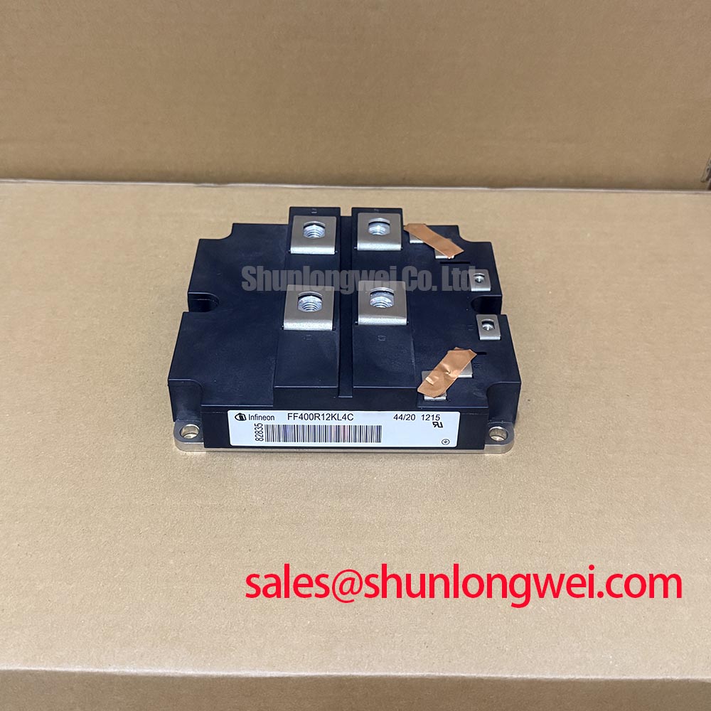
For a service replacement review, engineers can compare the mechanical and electrical interface requirements with FF400R12KL4C as a separate, neutral compatibility reference. Pin arrangement, gate-drive behavior, thermal interface, and protection settings must be checked before any substitution is considered.
Transient Dynamics and Four-Quadrant Power Flow in FF400R12KE3_B2
Four-quadrant PCS operation reverses both current direction and power direction as the inverter moves between battery charging, battery discharge, grid support, and regenerative conditions. The FF400R12KE3_B2 therefore needs to be evaluated inside the complete switching leg, not as an isolated current number. Peak shaving can create repeated thermal swings when high battery C-rate operation changes rapidly between active power flow directions.
Design consideration: separate the electrical review from the thermal review. The switching loop should be arranged to limit parasitic inductance and suppress turn-off overshoot, while the thermal interface should provide even pressure across the module baseplate. Gate-drive return paths should remain controlled during both current directions, and dead time, interlock behavior, desaturation response, and fault reset should be validated with the actual PCS controller.
For the thermal interface, a controlled layer of thermal interface material is commonly evaluated in the 50 to 80 µm range as an Engineering Recommendation, not as an Infineon factory specification for this module. The final thickness depends on the material, surface condition, flatness, application method, and compression. Excess compound can increase thermal resistance, while insufficient coverage can leave air pockets below the baseplate.
Mounting should follow a diagonal cross-pattern sequence so pressure develops progressively rather than loading one corner first. The applicable screw torque is a mechanical-system parameter that must come from the module documentation, fastener grade, heatsink design, and approved assembly procedure. After installation, inspect the contact pattern or use the approved process control method to confirm that the baseplate is seated evenly.
When the PCS includes an active front end or rectifier stage, the surrounding topology should be reviewed as a complete energy path. A related device such as BSM100GB120DLC may be evaluated as a separate front-end or complementary-stage reference, subject to voltage, current, gate-drive, and mechanical compatibility checks.
Bench Tip: Use ESD protection, discharge the DC link fully, and establish a cold-state baseline against a known-good module before connecting the gate-drive harness.
FF400R12KE3_B2 Circuit Protection and Auxiliary Emitter Return Layout
Keep the auxiliary emitter return electrically distinct from the main high-current emitter path when the gate driver uses a separate control reference. Shared impedance between these paths can create emitter feedback, ground bounce, and apparent gate-voltage distortion during fast current transitions. This is a Design Consideration for the complete converter layout, not a separately stated factory parameter of the module.
The gate-driver return should follow the intended control reference directly and should not be routed through copper carrying the principal emitter current. Place the driver supply decoupling and protection network close to the driver output interface, then verify the reference potential at the module terminals during switching. The objective is to prevent the driver from interpreting power-path voltage movement as a command signal.
Negative gate turn-off bias may be used in some industrial gate-drive systems, but its value, timing, and suitability are system determined. Designers should verify the permitted gate-emitter limits, driver isolation behavior, common-mode transient response, and fault-clamp operation from the applicable documentation. A negative bias should not be introduced as a universal remedy for oscillation.
Use the Infineon IGBT Paralleling Application Note when evaluating shared-current layouts or parallel module behavior. The return path, gate loop, emitter connection, and switching symmetry should be assessed together. During troubleshooting, probe the gate-emitter voltage at the module terminals rather than measuring only at the driver board.
Protection coordination should include overcurrent detection, short-circuit response, gate clamping, DC-link discharge control, and fault latching. If a phase shows intermittent trips, inspect the auxiliary return routing, connector contact condition, driver reference integrity, and switching waveform before changing protection thresholds.
FF400R12KE3_B2 Thermal and Electrical Optimization at the Heatsink Interface
Inspect the copper baseplate and heatsink contact surfaces for contamination, burrs, local distortion, and uneven seating before applying thermal compound. Surface flatness is a mechanical Design Consideration because a module rated at 400.0 A can still experience localized thermal stress if the heat path is poorly coupled. The inspection should cover the full contact area rather than only the screw locations.
Apply the selected thermal interface material consistently across the usable baseplate area. The previously noted 50 to 80 µm range is a Typical Starting Point for process evaluation, not a guaranteed FF400R12KE3_B2 specification. Measure the result through the approved production method and verify that the compound does not contaminate terminal insulation, mounting holes, or connector surfaces.
Tighten the mounting hardware in a diagonal sequence with calibrated tooling. The final torque must be taken from the applicable installation documentation and matched to the heatsink, fastener, washer, and thread condition. Recheck the assembly for rocking, corner lift, or visible compound displacement. A fractured substrate, damaged mounting boss, or distorted baseplate requires controlled inspection before energization.
Thermal validation should use the actual PCS duty profile, including charge, discharge, reactive-power support, regenerative braking, and idle transitions where applicable. Monitor case temperature, coolant or heatsink temperature, gate-drive status, and phase-current balance. A temperature rise may result from switching loss, conduction loss, interface resistance, current imbalance, airflow restriction, or control timing, so the recorded waveform and thermal data should be reviewed together.
For longer-term engineering reference, the Power Electronics Masterclass provides broader guidance on IGBT selection, system reliability, thermal paths, and switching evaluation. The final PCS release decision remains dependent on measured electrical margins, validated protection behavior, mechanical workmanship, and the intended operating profile.