

Content last revised on November 18, 2026
Assembly Integrity & Layout Architecture: Evaluating Commutation Ringing on 1MBI400VF-120-50
With the DC link isolated and verified discharged, disconnect the gate-driver connection before comparing cold collector-emitter and gate-emitter readings on the 1MBI400VF-120-50 against the equipment service procedure. Record meter polarity and disconnect parallel circuit paths where necessary; readings taken through a connected snubber, driver, or adjacent switch can obscure the condition of the module itself.
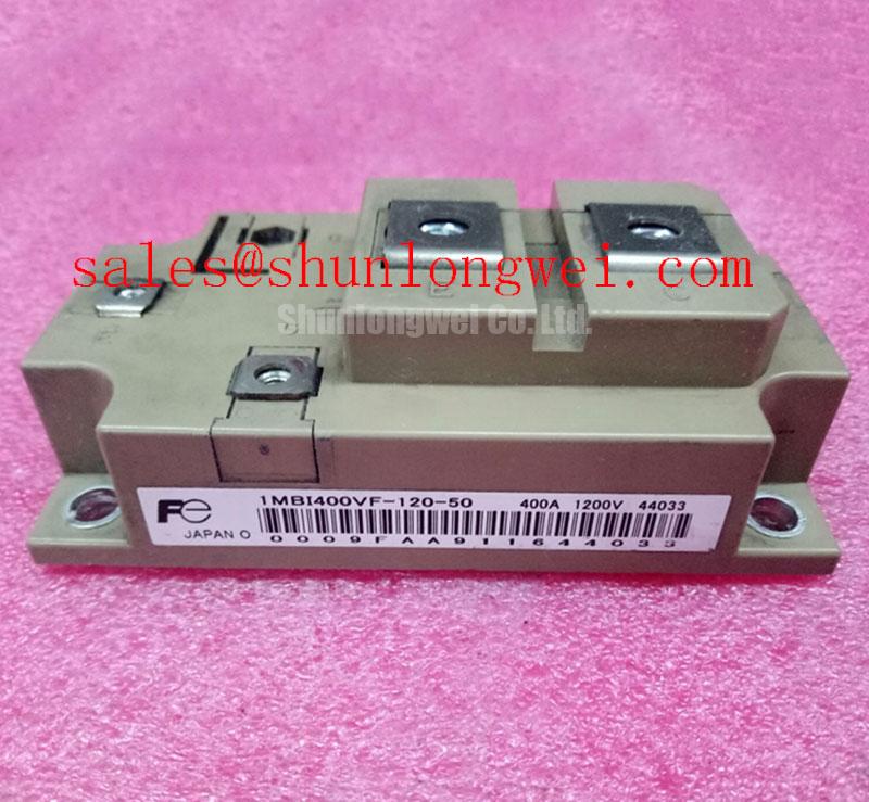
The product identification is Manufacturer: Fuji Electric; Part Number: 1MBI400VF-120-50; Collector-Emitter Voltage (Vces): 1200.0 V; and Continuous Collector Current (Ic): 400.0 A. Its specified Package: Fuji Power Module and Configuration / Topology: IGBT Power Stage describe a 1-in-1 Single Switch IGBT in the 6th Gen V-Series. These electrical ratings identify the device, rather than establish the repaired assembly’s operating current. Consult the model datasheet for rating conditions, terminal assignments, switching characteristics, and mechanical limits before substitution.
Capture collector-emitter voltage and commutating current together to distinguish diode reverse-recovery ringing from the IGBT turn-off current tail. As a Design Consideration, these are different switching phenomena: recovery occurs as a conducting freewheeling diode becomes reverse biased, while tail current follows IGBT turn-off. Treating every oscillation as tail current can send the repair toward the wrong gate resistor or snubber branch.
For the diode participating in the commutation path, evaluate peak reverse-recovery current, I_rrm, and the abruptness of its decay under representative temperature and current conditions. A sharp current collapse can excite the surrounding parasitic inductance and capacitance. Check probe placement and measurement bandwidth before attributing an apparent spike to the semiconductor; a long measurement loop can introduce ringing that is absent at the terminals.
As an Engineering Recommendation, inspect the physical commutation loop before changing damping components. Keep outgoing and return power paths closely coupled, preserve the intended laminated-busbar geometry, and check for displaced insulating sheets or loose overlapping joints. Required electrical clearances depend on the equipment’s insulation coordination and installation conditions, not on a spacing inferred from the module voltage rating alone.
If waveform evidence supports a change, the system designer can evaluate turn-on gate resistance or an RC snubber against recovery stress, switching loss, and component heating. Compare captures under equivalent conditions rather than selecting damping from waveform appearance alone. Fuji Electric’s 7th-Gen X-Series IGBT Modules information provides manufacturer context for a different generation; its characteristics must not be transferred to this V-Series part.
1MBI400VF-120-50 Circuit Protection & Reliability: Calibrating Floating Gate Bias Supply Decoupling
Check the floating driver supply at its local decoupling connection while observing gate-emitter voltage during enable, disable, and auxiliary-supply interruption. As a Design Consideration, a satisfactory unloaded supply reading does not demonstrate stable gate bias during switching. Excessive supply-path impedance, a degraded capacitor, or a disturbed driver return can change the voltage actually delivered to the gate.
Where the equipment uses negative turn-off bias, verify the approved bias level and its sequencing against the driver and module documentation. Do not select a negative voltage from a generic IGBT range. The control sequence should keep switching inhibited until the driver rails and undervoltage-lockout interlocks are valid, and should maintain the intended off-state control as the DC link discharges. Test these transitions through the equipment’s approved commissioning procedure.
Trace the auxiliary supply separately from the main power path when an intermittent trip follows driver enable. The guide to DC-DC converter modules in industrial and telecom applications provides supporting context for this auxiliary-power investigation. At the assembly, compare supply behavior at the converter output and driver input to distinguish distribution problems from a local load disturbance.
Protection coordination also requires more than matching fuse current to the module’s collector-current rating. As an Engineering Recommendation, assess semiconductor-fuse clearing I²t, interrupting capability, prospective fault current, and the manufacturer’s applicable withstand information alongside driver fault detection and shutdown behavior. A fuse can interrupt the fault path without necessarily preserving the IGBT. Review the actual protection sequence and energy exposure rather than assuming rapid clearing guarantees device survival.
Benchtop Waveform Tuning: Mitigating Stress via Gate Drive Resistance Calibration on 1MBI400VF-120-50
Record the installed turn-on and turn-off resistor network before disconnecting a legacy driver board, including any diode-steered branches and parallel resistor positions. As a Design Consideration, matching resistance markings does not establish equivalent switching behavior: driver output impedance, interconnect inductance, and the replacement device’s gate characteristics also affect the resulting waveform.
Route the gate connection and its emitter reference as a compact signal loop, away from the main switching-current path. Where the documented terminal arrangement provides an auxiliary emitter connection, use it according to that arrangement rather than allowing the gate return to share an avoidable power-current segment. This is a layout principle, not a claim that an undocumented terminal has a Kelvin-emitter function.
During controlled testing, compare gate-emitter excursions, collector-emitter overshoot, current transitions, and switching-loss trends. Increasing turn-on resistance can soften commutation but increase switching loss; changing turn-off resistance affects both voltage stress and shutdown behavior. Adjustments should therefore follow measured system behavior, including the driver’s protection response, rather than a universal resistance prescription.
For cross-model assessment, compare the 1MBI400U-120 with the required terminal map, mounting geometry, gate-drive conditions, thermal interface, and switching characteristics. It is a comparison candidate, not an automatic substitute. For potential integration into a utility-scale centralized battery energy storage PCS, designers should also verify bidirectional commutation requirements and the existing converter protection strategy.
Assess the 1MBI2400VD-170E separately if it appears elsewhere in the equipment’s power-conversion architecture; its circuit role must come from the schematic, not an assumption that it is a front-end rectifier or compatible companion. Likewise, Fuji Electric’s RC-IGBT module information concerns another device family and does not establish this model’s diode integration or replacement compatibility.
Assembly Integrity: Mitigating Mechanical Stress on 1MBI400VF-120-50
Check terminal-screw engagement against the module drawing and the complete lug, busbar, and washer stack before tightening. As a Design Consideration, a screw can reach the bottom of a threaded opening before it develops the intended clamping force. Conversely, insufficient engagement can leave a joint mechanically insecure even when the assembly initially conducts normally.
Support the busbar independently and align its contact surfaces without using the module terminals to pull it into position. Mechanical preload from a misaligned conductor can remain after tightening and change as the assembly heats. This supports an external assembly check; it does not establish the internal leadframe construction or diagnose an internal crack from appearance.
Field Alert: Do not use terminal screws to draw a misaligned busbar into place; correct the alignment before applying the documented tightening procedure.
Inspect the heatsink contact surface and remove old interface residue without damaging the mating surfaces. As an Engineering Recommendation, apply the specified thermal-interface material with controlled, even coverage and follow the documented mounting sequence. Interface thickness, fastener torque, and washer arrangement should follow the approved assembly specification rather than generic values borrowed from another housing.
After assembly, inspect for lifted lugs, displaced washers, trapped insulation, and conductor strain at the terminal interfaces. During authorized load testing, compare joint temperature patterns at equivalent current and cooling conditions; an elevated connection temperature warrants checking contact condition and clamping integrity. Record the final fastener configuration, interface material, and inspection results so a subsequent repair can reproduce the assembly rather than guess at its mechanical setup.
