



Content last revised on September 10, 2026
Optocoupler vs Digital Coreless Transformer Isolation in High-Voltage Switching
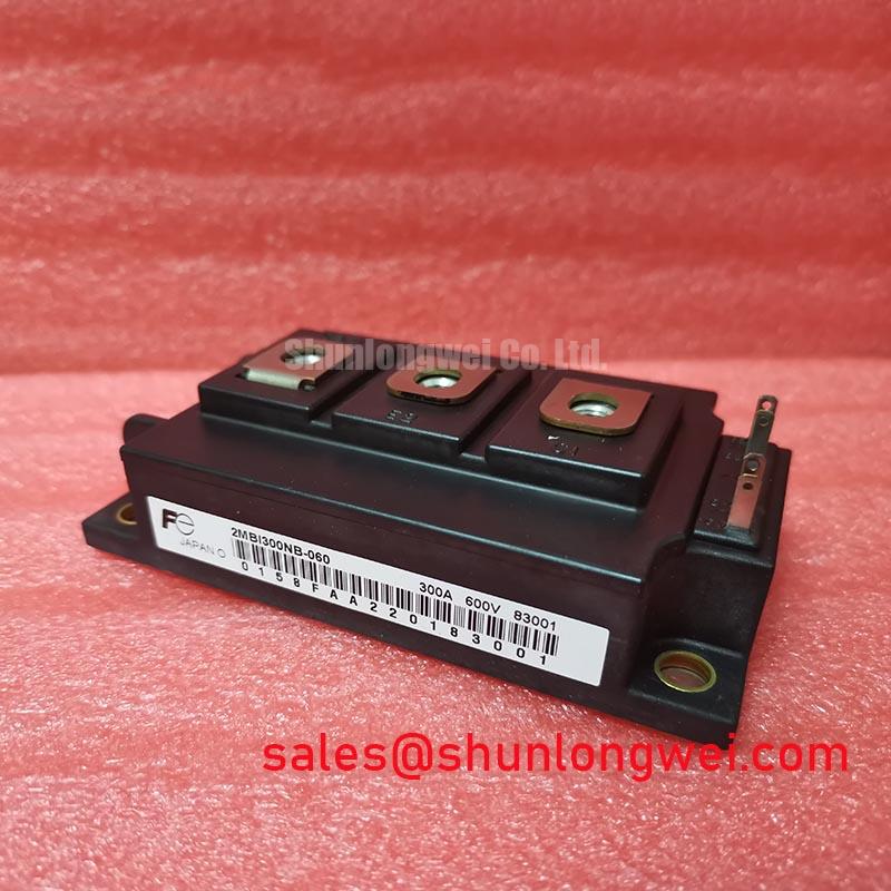
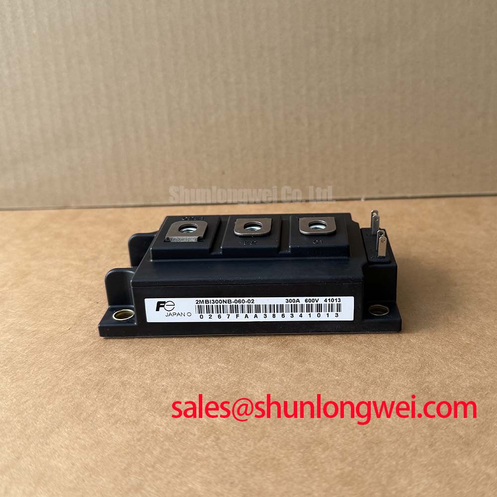
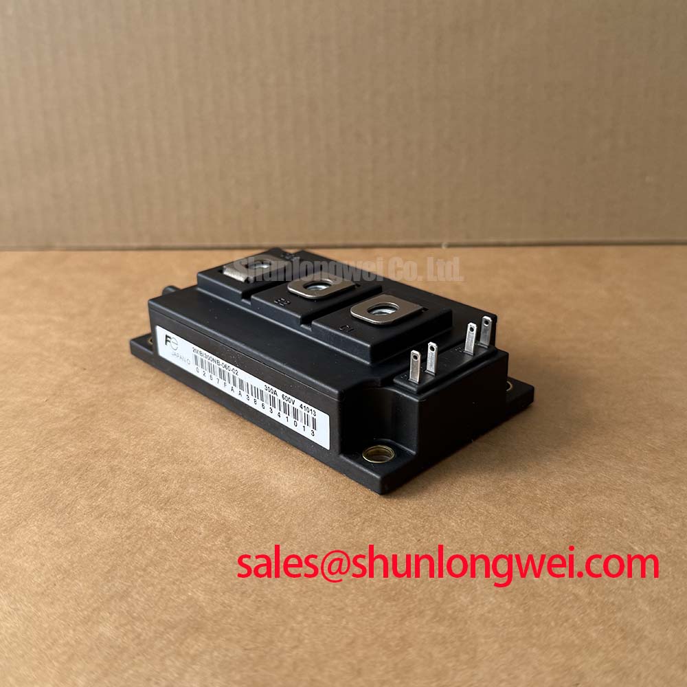
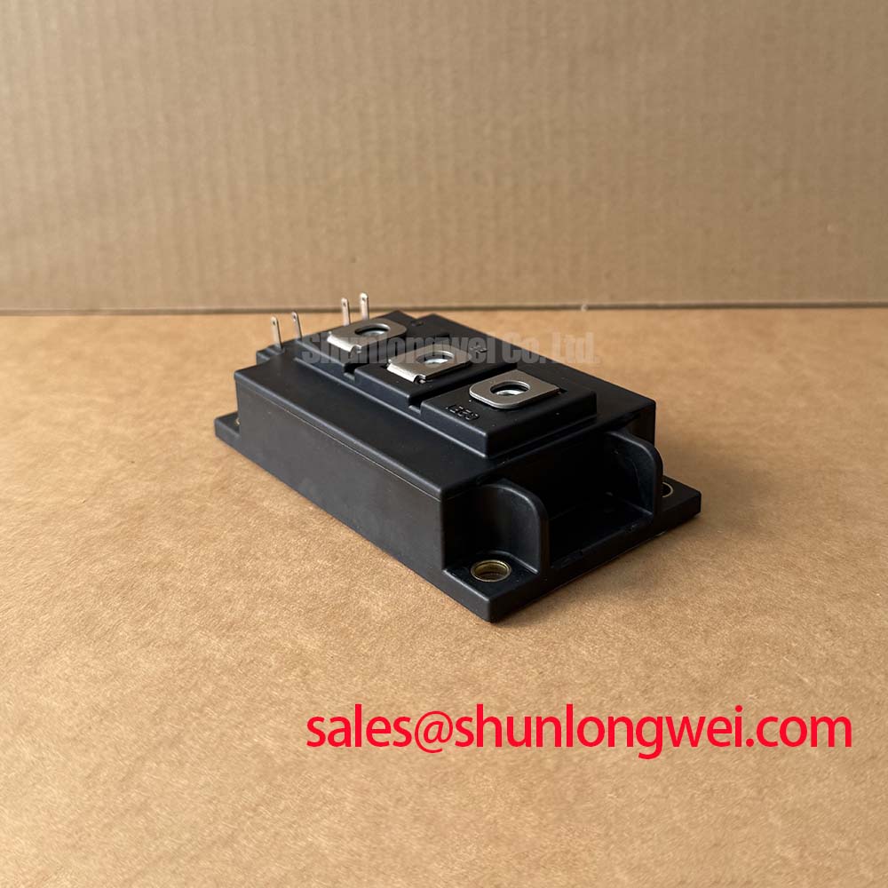
Field failures in commercial string inverters and battery energy storage systems (BESS) frequently trace back to driver-stage isolation degradation rather than direct silicon breakdown. When commissioning or servicing central power conversion units utilizing the Fuji Electric 2MBI300NB-060-02 dual IGBT module, isolation integrity between the high-voltage collector-emitter power path and the low-voltage microcontroller logic demands rigorous verification. The module provides a factory isolation rating of Viso = 2500V AC for 1 minute (Official Datasheet Specification), but maintaining signal barrier health under continuous multi-kilohertz pulse-width modulation requires careful scrutiny of driver technology.
Traditional industrial topologies often deploy high-speed optocouplers to cross the galvanic barrier. While optocouplers provide robust galvanic separation and high working DC voltage withstand, the aging curve of their internal gallium arsenide (GaAs) infrared light-emitting diodes presents maintenance challenges in continuous-duty micro-grid environments. Current transfer ratio (CTR) degradation over tens of thousands of operating hours reduces switching margins, gradually increasing propagation delay and propagation delay jitter. This drift skews the dead-time margins programmed into inverter bridge legs, elevating the risk of shoot-through events. Furthermore, standard optical isolators exhibit common-mode transient immunity (CMTI) thresholds often hovering around 15 kV/µs to 50 kV/µs. During sharp turn-off transients under high current, transient common-mode noise couples directly through the parasitic capacitance of the optical barrier, injecting spurious displacement currents into the gate driver output stage.
Modern retrofit designs and robust industrial platforms increasingly replace legacy optical couplers with galvanic digital coreless transformer isolators. These solid-state isolation barriers regularly exceed 100 kV/µs to 150 kV/µs CMTI, rendering gate control impervious to high transient switching voltages generated across busbars. In industrial installations where analog DC bus sensing and phase current monitoring share the same physical PCB assembly, utilizing high-precision isolation components such as Broadcom Optically Isolated Amplifiers & Current Sensors preserves signal fidelity while keeping hazardous bus voltages strictly partitioned from digital processing sub-racks. Isolating ground return paths and preventing ground loops through single-point chassis terminations represents a foundational layout practice documented in standard engineering literature on Ground Loop Isolation and Star Grounding Topologies.
A primary failure mechanism observed during bench diagnostics involves displacement currents charging the gate through the reverse transfer capacitance, or Miller capacitance (Cres). As the opposing switch in a half-bridge branch commutates, the rapid rise in collector-emitter voltage across the non-conducting 2MBI300NB-060-02 injects a current directly through Cres toward the gate terminal. If the gate driver output impedance is insufficient, this dynamic charge pulls the gate voltage above the threshold conduction level, inducing cross-conduction. Mitigating this risk requires dedicated active Miller clamping circuits. An active clamp transistor monitors gate voltage during the off-state; the moment gate potential falls below approximately 2.0V relative to the emitter, a low-impedance path directly shorts the gate terminal to the negative bias rail (such as -5V or -8V), effectively bypassing the external turn-off gate resistor and sinking the induced Miller displacement current harmlessly away from the internal channel.
Kelvin Emitter Connection & Parasitic Inductance Minimization in High-Speed Switching
The internal architecture of the Fuji Electric 2MBI300NB-060-02 integrates two distinct IGBT switches configured as a half-bridge, rated for a continuous collector current of IC = 300A at a baseplate temperature of 80°C (Official Datasheet Specification), with a repetitive peak capability of ICP = 600A for 1 millisecond. Switching hundreds of amperes in microsecond timeframes—where maximum turn-on time reaches ton = 1.20µs and maximum turn-off time is toff = 1.00µs (Official Datasheet Specification)—generates substantial di/dt rates within the internal bonding wires and external terminal leads.
Every millimeter of conductor inside the module and along the PCB traces introduces parasitic stray inductance. When power current flows through the primary emitter terminal, the rate of current change produces an induced back-electromotive force across the emitter's internal parasitic inductance. Because standard control circuits connect the gate drive return path to the emitter, this induced voltage directly opposes the applied gate driving voltage. During turn-on, the positive rate of change in collector current induces a negative voltage across the emitter inductance, which subtracts from the applied gate voltage, slowing the switching transition and increasing turn-on switching loss. Conversely, during turn-off, the rapid decline in current induces a positive voltage that artificially prolongs the conduction phase, creating severe gate ringing and potential latch-up.
To eliminate this destructive mutual inductive coupling, the physical wiring must strictly separate the auxiliary Kelvin emitter terminal from the main high-current emitter power return. The Kelvin emitter provides an independent potential reference dedicated exclusively to the gate driver loop. By routing the gate driver's return path directly to this auxiliary terminal, zero power-circuit load current traverses the control loop. Field technicians performing inverter card replacements must verify that auxiliary gate and emitter control cables are arranged as tightly twisted pairs or routed on adjacent PCB layers directly from the driver output stage to the control pins of the module. This physical layout minimizes the enclosed magnetic loop area, drastically attenuating externally induced electromagnetic interference.
When assessing system modularity or replacing legacy modules across varied drive architectures, technicians encounter different internal topologies and terminal layouts. For systems requiring discrete single-switch configurations rather than dual-pack half-bridge structures, evaluating the electrical parameters of single-device alternatives like the 1MBI300L-060 assists in selecting correct driver pinout configurations and mechanical bus spacing. Regardless of packaging style, keeping gate drive loops physically isolated from high-current DC link busbars remains mandatory to avoid parasitic inductive pickup that triggers unwanted switching oscillation.
Symmetrical Busbar Geometry for High-Current Parallel Module Arrays
Large-scale commercial string inverters and energy storage power conversion systems (PCS) frequently operate parallel half-bridge assemblies to deliver continuous power ratings running into hundreds of kilowatts. Operating modules in parallel presents critical challenges in static and dynamic current sharing. Statically, the collector-emitter saturation voltage governs current distribution across parallel legs. For the 2MBI300NB-060-02, the maximum saturation voltage is specified at VCE(sat) = 2.80V at the full rated current of 300A (Official Datasheet Specification). Because modern silicon designs demonstrate a positive temperature coefficient at nominal to high operating currents, an individual module carrying disproportionate current heats up, naturally elevating its internal saturation voltage and shifting excess load current toward neighboring parallel devices. However, this thermal equilibrium mechanism operates slowly and cannot prevent instantaneous dynamic current imbalances during switching edges.
Dynamic current balance relies entirely on electrical symmetry within external busbar geometries and gate drive distribution networks. If one module experiences lower parasitic loop inductance to the DC link capacitors, its collector current will ramp significantly faster during turn-on than its parallel counterpart. This imbalance subjects the lower-inductance module to severe turn-on current spikes, occasionally pushing peak instantaneous current beyond the pulsed rating of ICP = 600A. To enforce balanced dynamic sharing, field engineers and system assemblers must employ planar laminated busbar arrangements. Stacking positive (DC+) and negative (DC-) busplates separated by thin high-dielectric insulation sheets maximizes magnetic flux cancellation, minimizing total stray inductance down to tens of nanohenries across the intermediate DC bridge.
Dynamic balancing also extends directly to the complementary freewheeling diodes. The integrated fast recovery diodes inside the 2MBI300NB-060-02 feature a junction-to-case thermal resistance rated at Rth(j-c) = 0.24°C/W, compared to Rth(j-c) = 0.11°C/W for the main IGBT switch (Official Datasheet Specifications). During high-frequency commutation, diode reverse recovery current behavior influences high-frequency EMI generation. A diode exhibiting a snappy reverse recovery characteristic experiences an abrupt drop in reverse current, which rings with busbar parasitic inductance to generate high-frequency radiated and conducted noise. In contrast, soft-recovery profiles ensure that current drops smoothly back to zero, attenuating voltage overshoot and reducing common-mode interference.
System designers and field teams evaluating alternative modules within similar voltage and current classes often cross-reference legacy products such as the 2MBI300J-060 to compare switching characteristics, gate charge curves, and thermal impedance metrics. Matching gate loop wire lengths down to the millimeter across parallel modules ensures synchronized switching timing, preventing one module from prematurely absorbing full bridge commutation energy during critical turn-off transition intervals.
Baseplate Thermal Grease (TIM) Layer Control & Heatsink Mounting Torque Optimization
Thermal management dictates whether an industrial power module survives continuous high-current cycles or suffers premature baseplate solder fatigue. The copper baseplate of the 2MBI300NB-060-02 is manufactured with an intentional convex curvature. When unmounted, the center of the module baseplate bows outward slightly relative to its mounting tabs. This intentional mechanical crown compensates for the microscopic deflection that occurs when mounting bolts pull down on the perimeter flange against a flat liquid-cooled chill plate or extruded aluminum heatsink.
Applying thermal interface material (TIM) requires precise thickness control. Field technicians frequently make the mistake of applying an excessively thick grease layer, assuming more thermal compound enhances heat transfer. In reality, standard silicone or non-silicone thermal compounds possess thermal conductivities ranging between 1.0 W/m·K and 4.0 W/m·K, whereas direct metal-to-metal contact with copper exhibits a conductivity exceeding 380 W/m·K. An overly thick grease layer introduces severe thermal impedance, drastically raising junction temperature under steady-state load.
The optimal applied TIM thickness before compression should measure strictly between 50 µm and 100 µm (General Industry Design Consideration). Applying grease using a calibrated stainless steel screen stencil or a high-precision notched roller ensures an even, repeatable distribution across the entire surface. If applied manually with a spatula, technicians must ensure no air bubbles, debris, or lint are trapped within the layer. When the module is mounted, mechanical pressure spreads the thermal compound from the center outward toward the perimeter edges, displacing trapped air voids and filling microscopic surface asperities on the heatsink surface.
⚠️ Field Alert: Never torque mounting screws to their final setting in a single pass. Uneven single-step torque application tilts the module baseplate, creating permanent mechanical distortion, cracking internal direct bonded copper (DBC) ceramic substrates, and squeezing thermal grease completely out of one corner while leaving massive air voids under the opposing switch. Always follow a strict cross-pattern two-stage torque sequence:
- Stage 1 (Pre-Torque): Hand-thread all M5 baseplate mounting bolts, then lightly snug them in a crisscross diagonal pattern (Screw 1 -> Screw 4 -> Screw 2 -> Screw 3) to a preliminary torque of approximately 0.5 N·m (General Industry Design Consideration). This allows the thermal grease to settle and begin outward displacement without tilting the copper base.
- Stage 2 (Final Torque): Allow 5 minutes for viscous TIM relaxation, then torque the fasteners to the specified final mounting value—typically 2.5 N·m to 3.5 N·m for standard M5 hardware into tapped heatsinks (General Industry Design Consideration)—following the exact same diagonal sequence.
- Stage 3 (Terminal Torque): Secure the main power busbars to the M6 electrical terminals using a calibrated torque wrench set to 3.5 N·m to 4.5 N·m (General Industry Design Consideration). Ensure busbars sit perfectly flush against terminal surfaces without mechanical leverage or angular misalignment that exerts constant prying forces on terminal plastic frames.
Before energizing any repaired inverter sub-assembly, technicians should conduct standardized multimeter screening protocols. With gate drivers disconnected, measure gate-emitter resistance; the resistance should read infinite (open-circuit) on high-resistance ranges. Any reading below several megaohms indicates gate oxide puncture. Next, perform a diode-check measurement across collector-emitter terminals to verify freewheeling diode forward voltage drop (typically 0.35V to 0.7V depending on multimeter test current) and verify zero reverse conduction. For exhaustive root-cause investigation protocols, gate leakage testing methods, and reliability qualification standards under severe industrial vibration and cycling, reference the diagnostic guides compiled in the Field Engineer’s Handbook.
Critical Engineering Specifications Reference
| Parameter Group | Technical Symbol & Description | Datasheet Specification | Engineering Identity |
|---|---|---|---|
| Maximum Ratings | Collector-Emitter Voltage (VCES) | 600V | Official Datasheet Specification |
| Maximum Ratings | Gate-Emitter Voltage (VGES) | ±20V | Official Datasheet Specification |
| Continuous Current | Collector Current (IC @ TC = 80°C) | 300A | Official Datasheet Specification |
| Pulsed Current | Peak Collector Current (ICP, 1ms) | 600A | Official Datasheet Specification |
| Galvanic Isolation | Isolation Voltage (Viso, AC 1 min) | 2500V AC | Official Datasheet Specification |
| Saturation Conduction | Collector-Emitter Saturation Voltage (VCE(sat) @ 300A) | 2.80V (Max) | Official Datasheet Specification |
| Switching Speed | Turn-On Time (ton) / Turn-Off Time (toff) | 1.20µs / 1.00µs (Max) | Official Datasheet Specification |
| Thermal Impedance | Thermal Resistance – IGBT Junction-to-Case (Rth(j-c)) | 0.11°C/W (Max) | Official Datasheet Specification |
| Thermal Impedance | Thermal Resistance – Diode Junction-to-Case (Rth(j-c)) | 0.24°C/W (Max) | Official Datasheet Specification |
| Installation Parameters | Heatsink Mounting Torque (M5 Hardware) | 2.5 – 3.5 N·m | General Industry Design Consideration |
| Installation Parameters | Thermal Interface Material Thickness | 50 – 100 µm | General Industry Design Consideration |