
Content last revised on September 15, 2026
Field Diagnostics & Commissioning: Evaluating Thermal Response and Heat-Sink Performance in PM150RRA060 Topologies
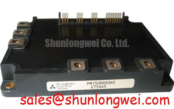
The PM150RRA060 from Mitsubishi Electric is rated at 600 V collector emitter voltage, 150 A collector current at TC = 25°C, 300 A peak collector current, and 500 W collector dissipation at TC = 25°C. These are Official Datasheet Specifications, not guaranteed operating conditions for every installed inverter. A heavy duty variable frequency AC motor drive must be assessed as a complete thermal system, including its switching pattern, current waveform, heat sink condition, enclosure airflow, thermal interface condition, and overload profile.
During commissioning, begin with the inactive system. Inspect the baseplate contact area for contamination, uneven thermal compound transfer, corrosion residue, or mounting distortion. A clean and planar interface supports repeatable heat transfer from the module baseplate into the heat sink. If a drive has experienced repeated overload trips or unexplained temperature alarms, do not assume that the semiconductor alone is responsible. Blocked airflow, a loose heat sink assembly, deteriorated compound, fan control faults, and unbalanced phase loading can all alter the measured thermal response.
The specified operating junction temperature range is −20 to +125°C as an Official Datasheet Specification. The usable junction temperature margin in a real drive must therefore be verified from measured case temperature, current duty, switching activity, and the applicable transient thermal impedance information. A multi RC thermal model can represent how heat moves through the internal thermal path over time, but a numerical peak junction estimate should not be invented when the required module specific transient thermal curves, switching loss data, and actual pulse profile are unavailable. Engineering Calculation requires those inputs.
For pulsed overload evaluation, capture the load current, DC bus voltage, switching frequency, heat sink temperature, and overload duration together. A short current pulse may not immediately produce a high baseplate temperature, while junction temperature can still rise quickly. Conversely, a hot baseplate reduces the available thermal headroom before the next load event. Compare measured operating behavior against a known healthy drive where available, and verify whether current limitation and thermal protection occur in the intended sequence.
Electrical clearances around the main terminals also need inspection after service. Conductive dust, carbon tracking, loose bus hardware, and displaced insulation barriers can create a high energy fault path without an obvious initial mechanical defect. The module has an Official Specification of 2500 Vrms isolation voltage for 1 minute between main terminals and baseplate. This rating does not replace the insulation coordination requirements of the finished equipment. Creepage distance, clearance, pollution level, enclosure conditions, and the protection system remain system level responsibilities.
⚠️ Field Alert: Disconnect, lock out, and verify discharge of the DC link before removing any power or gate connection from the PM150RRA060 assembly.
Transient Dynamics & Electrical Design: Switching Overshoot and Gate-Drive Considerations for PM150RRA060
The PM150RRA060 has a 600 V VCES Official Datasheet Specification, so switching overshoot must be assessed against the actual DC bus waveform rather than the nominal supply label. During turn off, stray inductance in the commutation path can add voltage overshoot as current changes. The practical design objective is to minimise loop inductance between the module, DC link capacitor, and commutating path, then verify peak collector emitter voltage with correctly referenced switching measurements under representative load conditions.
A compact, symmetric bus arrangement can reduce unequal current paths and limit the energy available to ringing. The appropriate margin is determined by the inverter topology, capacitor placement, cable arrangement, load current, switching conditions, clamp strategy, and measured transient waveform. A metal oxide varistor can be evaluated as part of an overvoltage absorption network where the system’s surge environment and coordination requirements support its use. It should not be treated as a substitute for controlling switching loop inductance or for validating the module voltage waveform.
Design Consideration: terrestrial neutron exposure and altitude related single event effects require evidence from the applicable device qualification data, system mission profile, and environmental standard before any reliability rate is stated. No module specific FIT rate, single event burnout rate, altitude derating curve, or operating lifetime figure is asserted here. For equipment intended for elevated locations, the system engineer should evaluate insulation coordination, cooling capability, DC bus headroom, and environmental requirements using the relevant equipment documentation and measured operating conditions.
Where the inverter uses a floating high side driver with bootstrap power, capacitor sizing should account for the actual gate charge, driver quiescent current, leakage paths, refresh interval, allowable driver supply variation, and duty cycle. Those values must be taken from the installed gate driver and module documentation. The high side supply must be checked during the longest practical on interval and through switching transients, rather than selected from a generic capacitor value. The Mitsubishi DIPIPM™ Bootstrap Circuit Design note provides useful general background for bootstrap circuit evaluation, while the actual PM150RRA060 gate drive implementation must be verified against its applicable documentation.
Gate turn off behavior deserves particular attention when common mode voltage moves rapidly. A negative turn off bias can be considered as a Design Consideration where the selected gate driver and module limits permit it, because it can increase immunity to unintended turn on caused by Miller coupling. Its final value, gate resistance, clamp arrangement, and driver voltage rating must be determined from the complete gate loop and validated on the bench. There is no universal drive prescription that can safely be transferred between inverter layouts.
PM150RRA060 Circuit Protection & Reliability: Calibrating Derating Guidelines and Mismatched Parameters
A drive using the PM150RRA060 should be evaluated against all published electrical and thermal limits, not only the 150 A collector current rating. The 300 A peak collector current rating is an Official Datasheet Specification and must not be interpreted as an indefinitely available overload current. Actual peak current capability depends on pulse duration, junction temperature, switching conditions, protection response, DC link behavior, and the safe operating limits stated in the applicable manufacturer documentation.
For parallel current paths, static current distribution and switching current distribution are different problems. IGBT conduction characteristics can show a positive temperature coefficient in relevant operating regions, which can assist steady state sharing under controlled conditions. It does not guarantee balanced current during turn on and turn off. Differences in gate resistance, driver propagation timing, gate return routing, main conductor impedance, thermal path, and parasitic inductance can cause dynamic imbalance even when components appear electrically similar at rest.
Engineering Recommendation: keep corresponding gate drive paths physically comparable, route each gate return with its associated gate conductor, and avoid allowing high current emitter paths to become part of the gate reference loop. Then confirm switching symmetry with voltage and current measurements under controlled conditions. If one phase shows abnormal ringing, gate waveform distortion, or inconsistent current behavior, investigate the complete commutation loop, driver supply integrity, busbar geometry, and sensing reference before assigning a single cause.
Protection coordination should be verified at the inverter level. Overcurrent detection, gate drive shutdown behavior, DC bus supervision, thermal monitoring, and controller fault handling must act in a sequence appropriate to the installed motor drive. A fast fault event can involve stored energy in cables, bus capacitors, and the motor circuit, so a gate command removal alone may not define the actual collector voltage and current trajectory. Oscilloscope measurements should use appropriate differential voltage and current probes with safe connection practices.
When a repair review requires comparison with another power module, electrical equivalence cannot be inferred from current rating alone. The CM300DXDX1-24A is a separate module that engineers may assess against the original circuit’s voltage class, topology, terminal arrangement, gate drive requirements, thermal interface, protection coordination, and mechanical fit. It is not presented as an automatic replacement for the PM150RRA060.
For broader context on IGBT switching behavior, thermal mechanisms, and system level evaluation methods, consult The Ultimate IGBT Knowledge Base. Any final repair or integration decision should remain anchored to the original inverter documentation, module datasheet, and measured system conditions.
PM150RRA060 Operational Boundaries: Evaluating Kelvin Emitter Connection Limits
Before connecting a gate driver, confirm the PM150RRA060 terminal designation and control pin assignment from the applicable module documentation and the original equipment schematic. Do not infer auxiliary terminal functions from package appearance or from another Mitsubishi Electric module family. A control connection that is incorrectly referenced to a main current terminal can produce misleading gate voltage measurements and unstable switching behavior.
Where the module and original circuit provide a dedicated auxiliary emitter or Kelvin emitter reference, its intended value is to provide the gate driver with a reference less affected by voltage developed in the main power emitter path. This is a Design Consideration based on common power module integration practice, not a claim about undocumented internal construction. The gate driver return should follow the designated control reference path, while the main emitter conductor carries the high current commutation path separately.
Mutual coupling occurs when the high current power return and low level gate return share unwanted impedance. During switching, this shared impedance can shift the apparent gate emitter voltage, encourage ringing, or alter the effective turn on and turn off response. Keep the gate loop compact, avoid long unpaired wiring, and prevent the gate reference from crossing noisy power conductors where layout permits. The correct arrangement must be verified on the installed hardware because busbar geometry, driver location, shielding, and control grounding all influence the result.
Common mode ground movement can also disturb current sensors, control interfaces, and isolated driver communications. Shielding and reference strategy should be evaluated as part of the complete inverter architecture. A shield connection that improves one noise path can worsen another if it creates an unintended return route. Verify suspected noise coupling with measurements referenced to a known good signal path, then adjust the system layout or interface treatment according to the observed behavior and the original equipment requirements.
For a heavy duty variable frequency AC motor drive, commissioning should include controlled checks of gate emitter waveforms, collector emitter transients, phase current balance, protection response, heat sink temperature progression, and insulation condition. These checks establish whether the 600 V, 150 A PM150RRA060 is operating inside the boundaries supported by the actual drive, rather than relying on a single nameplate rating or visual inspection alone.



