
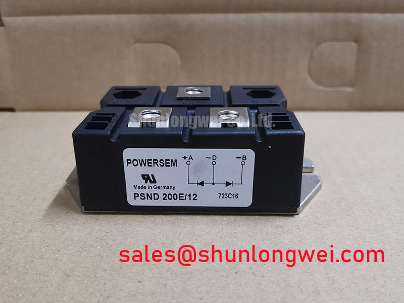
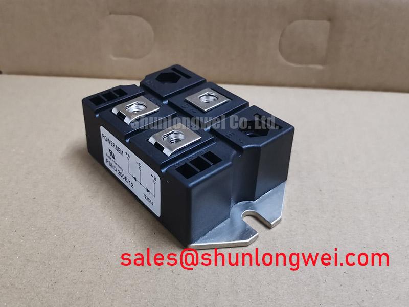


Content last revised on September 30, 2026
PSND200E-12 Circuit Protection and Reliability: Gate-to-Emitter Loop Routing
| Parameter | Specification |
|---|---|
| Model | PSND200E-12 |
| Manufacturer | Industrial Manufacturer |
| Product Category | Power Semiconductor Module |
| Package | Module |
Measure the gate-to-emitter and power-terminal relationships with the module unpowered, then compare the physical gate return path with the main high-current emitter route before applying a switching waveform. Available product information does not specify numeric voltage or current ratings, so those limits must be verified against the original equipment documentation.
As a Design Consideration, keep the gate drive loop compact and route its return independently from the high-current emitter path where the circuit topology provides that option. Shared copper can introduce common-emitter inductive coupling, which may appear during bench testing as ringing, uneven turn-off behavior, or a gate waveform that changes when collector current rises. Use an oscilloscope with an appropriate differential probe to compare the gate-to-emitter waveform at the module terminals rather than relying on a remote driver board test point.
For an Industrial Inverter Welder or Medium Frequency Induction Heating supply, verify terminal identity against the equipment schematic and the physical marking on the replacement module. A cold-state resistance comparison between a known-good assembly and the installed unit can reveal wiring or assembly discrepancies, but a resistance reading alone cannot validate switching performance. Designers should also check the driver isolation barrier, gate resistor network, and fault feedback path as a connected system.
Bench Tip: Use ESD controls and record the cold-state terminal measurements before connecting the gate driver, then repeat the comparison after mechanical installation.
For additional gate loop design context, see Precision Gate Drive Design.
Assembly Integrity and Layout Architecture: Evaluating DC Bus Voltage Doubling Effects
Probe the module terminals and the load side of the output connection during a controlled switching test to distinguish a local device transient from a reflection on a long motor or transformer lead. Long conductors can behave as transmission lines, and impedance discontinuities may produce overshoot that is not visible at the inverter control board.
This is an Engineering Recommendation rather than a factory specification for PSND200E-12. Minimize abrupt conductor changes, keep the outgoing and return paths closely coupled where the system permits, and place any dv/dt filter or choke according to the measured cable and load behavior. The filter selection must be determined from the actual DC bus, switching waveform, load impedance, insulation system, and thermal conditions. Confirm peak terminal voltage with a properly rated probe during the intended operating sequence.
Incoming inspection should verify the module terminal arrangement against the original wiring record before busbar fastening. Check creepage and clearance around energized conductors using the applicable equipment insulation requirements. Mechanical work should leave the terminals free from side loading, and busbars should remain supported so vibration does not transfer force into the module body or terminal interfaces.
Preventing Spurious Faults: DC Bus Low Inductance Busbar Design Guidelines
Capture the turn-off waveform directly across the switching path and compare it with the DC bus measurement when investigating a desaturation trip or unexplained overvoltage. The transient relationship can be considered through the engineering expression Vpeak equals VDC plus the stray inductance multiplied by the current change rate, but the acceptable peak is system determined and must be verified against the module rating and protection response.
Use a symmetrical planar busbar arrangement where practical, shorten the commutation loop, and position the relevant snubber or clamp network according to the measured current path. Do not treat a calculated inductance target as a PSND200E-12 factory parameter. The final geometry depends on conductor thickness, spacing, connection hardware, switching speed, and the physical placement of the DC link capacitor.
During troubleshooting, inspect fasteners, contact surfaces, laminated insulation, and signs of localized heating. Recheck the waveform after each physical change so that a reduction in ringing can be correlated with the changed current loop. An apparently acceptable static resistance test does not confirm low inductance during a high di/dt event.
Where the equipment uses semiconductor fuses, coordinate the fuse I²t characteristic with the module protection strategy and the system short-circuit response. This coordination is a Design Consideration; the available product information does not establish a short-circuit withstand time, fusing limit, or explosion prevention rating for this model.
Preventing Spurious Faults: Static and Dynamic Current Distribution
Measure current in each parallel branch and compare the gate waveforms at the module terminals when investigating unequal current distribution. If VCE(sat) has a positive temperature coefficient under the relevant operating conditions, it can support static sharing in appropriately matched power paths, but dynamic sharing remains sensitive to gate loop impedance, stray inductance, driver timing, and physical symmetry.
When multiple switching paths are used, match the conductor length and routing structure as closely as the equipment layout allows. Keep the gate drive reference consistent with the corresponding power return, and verify turn-on and turn-off timing on every branch under representative load conditions. These are Engineering Recommendations, not guaranteed characteristics of PSND200E-12.
Protection testing should include the desaturation or VCE monitoring circuit, soft turn-off behavior, fault latch timing, and isolation barrier response. The driver should be evaluated for common-mode transient immunity under the actual switching layout. A fault during this test may involve the gate driver, measurement circuit, busbar, load, or module, so compare the signal path against a known-good assembly rather than assigning a single cause from one symptom.
For lifetime assessments, separate measured power cycling data from calculated estimates. A Weibull model can describe a population distribution when supported by suitable test data, as outlined in Weibull distribution. No field failure rate or operating life value is established here for PSND200E-12.