

Content last revised on October 4, 2026
T640N14TOF Specifications and Incoming Inspection
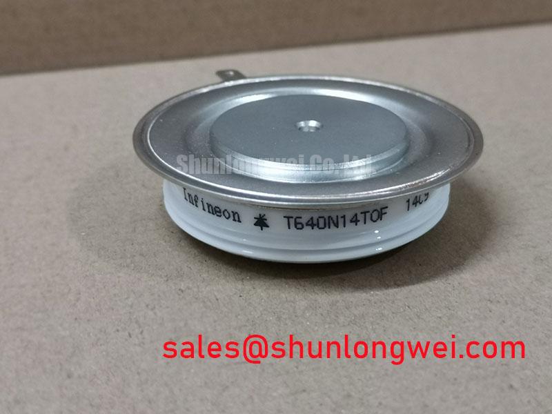
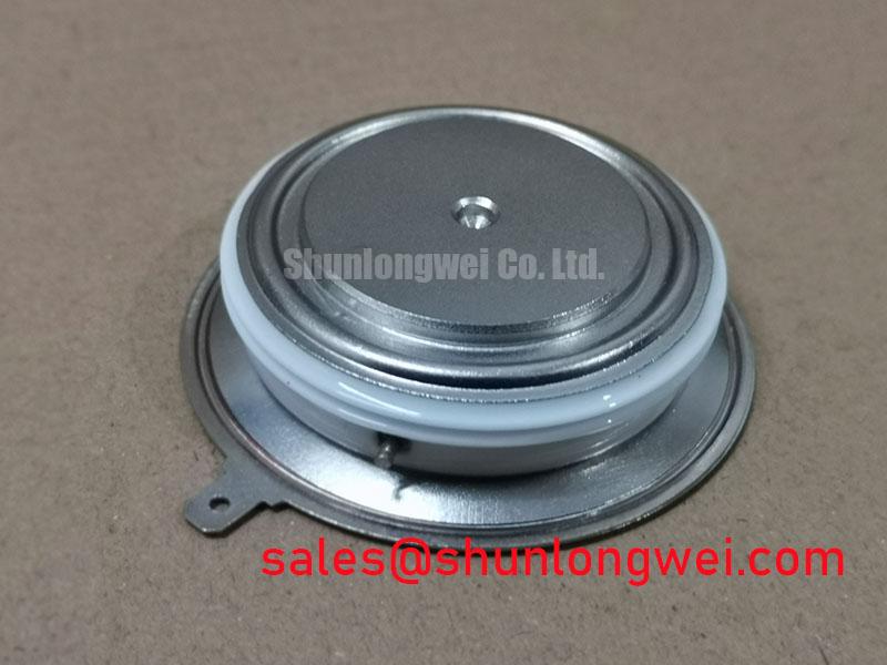
Begin incoming inspection by recording the marking, checking the PowerBlock Module housing for mechanical damage, and verifying the rated boundary of T640N14TOF before applying any test voltage. The supplied official specifications identify this Infineon Thyristor/Diode Module as rated at 1400.0 V and 690.0 A. The exact terminal arrangement, gate and auxiliary connections, fuse coordination data, thermal limits, and mounting requirements should be confirmed against the applicable manufacturer documentation before installation.
| Parameter | Official Specification |
|---|---|
| Manufacturer | Infineon |
| Product category | Thyristor/Diode Module |
| Package | PowerBlock Module |
| Rated voltage | 1400.0 V |
| Rated current | 690.0 A |
Transient Dynamics and Electrical Design for Primary Protection
For a grid-tied Static Var Compensator or thyristor-switched capacitor installation, the first design task is to coordinate the external protection network with the module’s confirmed voltage and current ratings. A primary spark gap, metal oxide varistor, semiconductor fuse, and RC snubber each address a different transient condition. Their voltage class, energy capability, response behavior, and installation location must be selected from the system fault study and the manufacturer’s coordination data rather than inferred from the module rating alone.
IEC 61000-4-5 may be used as a surge-test reference for the wider equipment, but the presence of a 1400.0 V rated device does not by itself demonstrate compliance with that standard or with the completed SVC assembly. Designers should verify clamping levels at the module terminals, prospective fault current, fuse clearing behavior, and repetitive switching stress during controlled tests. Keep the surge-current path physically separate from sensitive firing circuitry, and minimize parasitic loop inductance where turn-off overshoot is a concern.
The PowerBlock Module connection layout must be checked from the relevant drawing before busbar fabrication. Do not assume that an auxiliary or gate terminal has Kelvin behavior, polarity, or current capability unless it is explicitly defined. A replacement assessment should compare terminal geometry, electrical ratings, cooling interface, and the original fuse coordination table. The neutral TD210N12 reference can support cross-model evaluation, but it should not be treated as an automatic substitute for T640N14TOF.
T640N14TOF Thermal-Electrical Optimization During Commutation
Reverse-recovery behavior belongs to the complete commutation network, not to the headline current rating alone. When this module is evaluated in a controlled rectifier or capacitor-switching assembly, engineers should obtain the applicable diode reverse-recovery parameters, switching conditions, junction temperature assumptions, and repetitive current limits from the manufacturer’s technical documentation. Those values are needed to assess commutation loss, voltage overshoot, and possible EMI coupling.
Thermal evaluation should start with a clean mounting surface, an even pressure distribution, and a verified heatsink interface. The system designer must determine the allowable case temperature, cooling capacity, airflow or liquid conditions, and electrical duty cycle from the complete assembly requirements. A thermal camera can help locate abnormal temperature differences between parallel paths, while oscilloscope measurements can correlate heating with firing angle, current transfer, or recovery transients.
High-frequency gate wiring, any isolated driver supply, and local charging components should be routed according to the confirmed terminal definition. A bootstrap capacitor and its charging diode should not be added or sized by assumption; the integrator should verify whether that topology is appropriate for the selected firing circuit and whether capacitor ripple current and diode recovery remain acceptable at the operating frequency.
Circuit Protection and High di/dt Gate-Firing Coordination
Gate firing for a high-current thyristor assembly requires a controlled pulse source, a defined return path, and adequate isolation from the power commutation loop. The requested pulse-rise, gate-current, back-porch, and multipulse values are application parameters and must be taken from the applicable Infineon gate-trigger specifications for the exact device configuration. They are not established by the 1400.0 V and 690.0 A ratings alone.
During commissioning, verify gate-to-cathode polarity with the power stage isolated, then compare the firing waveform at the module terminals rather than only at the driver output. Oscilloscope checks should look for ringing, pulse distortion, ground-reference movement, and timing differences between parallel firing channels. Separate auxiliary returns from high-current power returns where the terminal design permits, and let the system engineer validate the resulting noise margin under the actual switching current.
💡 Bench Tip: Use ESD protection and compare cold-state terminal measurements with a known-good reference before connecting the firing harness or applying high voltage.
Infineon’s general information on qualified power modules and intelligent power modules can provide useful technology context, but neither page replaces the product-specific gate and protection data required for this module.
Operational Boundaries and Short-Circuit Coordination
A semiconductor fuse must be coordinated with the thyristor and diode withstand limits using the manufacturer’s published I²t data, fault-current waveform, clearing time, and prospective system impedance. The module’s 1400.0 V voltage rating and 690.0 A current rating are official product parameters, not a guarantee of safe operation during a dead short, abnormal commutation event, or uncontrolled surge.
For an SVC or thyristor-switched capacitor bank, the protection review should include capacitor discharge energy, reactor impedance, bus voltage, fuse interrupt rating, snubber condition, and isolation sequence. Confirm that the fuse coordination table applies to the intended duty and ambient conditions. If the required table or short-circuit withstand data is unavailable, the safe engineering action is to obtain the missing documentation and perform a controlled verification rather than assign a speculative clearing limit.
Use the The Ultimate IGBT Knowledge Base as a supplementary reference for power-semiconductor testing principles, while keeping the final installation decision tied to the applicable Infineon documentation, measured waveforms, and the completed protection study.