

Content last revised on September 26, 2026
J2-Q06B-G Field Identification and Electrical Boundaries
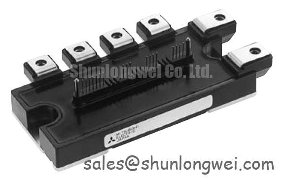
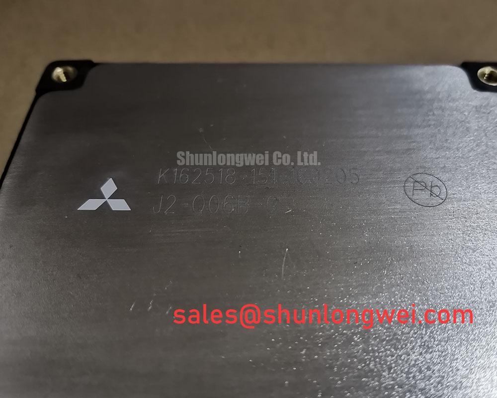
With the DC bus fully isolated and discharged, begin by recording the module marking, checking the case for cracks or deformation, and measuring cold-state impedance between the accessible power terminals against a known-good reference. Do not apply a control signal during this first inspection. The Fuji Electric J2-Q06B-G is identified in the supplied product data as a Power Transistor Module with a rated voltage of 600.0 V and a rated current of 20.0 A.
These supplied product ratings are useful for initial equipment assessment. They do not, by themselves, define the allowable DC-link operating point, switching frequency, short-circuit withstand time, surge current capability, thermal resistance, control-drive requirements, or safe operating area. The system integrator should verify those values from the original Fuji Electric documentation applicable to the exact device and circuit revision.
The supplied “Power Transistor Module” designation does not establish an insulated-gate device architecture. The gate-drive, Miller-effect, and gate-capacitance discussion below is conditional guidance for an insulated-gate switching stage, not confirmation of the J2-Q06B-G’s internal construction. If the original documentation identifies a bipolar transistor module, use its specified base-drive requirements and switching characteristics instead.
| Parameter | Specified Value | Engineering Use |
|---|---|---|
| Manufacturer | Fuji Electric | Confirm the replacement identity against the equipment bill of materials |
| Model | J2-Q06B-G | Use the complete ordering code during service procurement |
| Rated voltage | 600.0 V | Compare with the measured switching and DC-link voltage envelope |
| Rated current | 20.0 A | Compare with load current, duty cycle, cooling, and transient conditions |
| Device designation | Power Transistor Module | Check mechanical interface, terminal arrangement, and heatsink compatibility |
For an industrial inverter welder or medium-frequency induction heating power supply, replacement work should include a comparison of terminal geometry, busbar clearance, control-drive routing, cooling contact, and protection feedback. A module with the same voltage and current labels is not automatically a drop-in substitute if the drive characteristics, internal circuit arrangement, or mechanical interface differ.
Field Diagnostics and Commissioning: Regenerative DC-Bus Voltage Surge Dissipation in J2-Q06B-G Topologies
When the J2-Q06B-G is used in a switching stage connected to a regenerative DC bus, first separate the semiconductor inspection from the braking network inspection. Check the braking transistor path, ballast resistor connections, DC-link sensing circuit, discharge path, and contactor sequence before energizing the inverter. A failed resistor, open connection, incorrect feedback polarity, or delayed braking command can expose the power module to a voltage excursion that is not visible during a simple static resistance test.
The braking network must be dimensioned from the actual deceleration energy, repetition rate, DC-link capacitance, permissible bus voltage, resistor pulse rating, and semiconductor switching conditions. These values are system calculations, not published specifications for the J2-Q06B-G. During commissioning, designers should capture the DC-link waveform with a properly rated differential probe and verify the peak voltage at the module terminals during the fastest expected regenerative event. Layout inductance between the module, braking element, capacitor bank, and measurement point should be minimized to reduce measurement error and turn-off overshoot.
Short-circuit protection requires equal care. A desaturation or VCE(sat) monitoring circuit can support fault detection, but the threshold, blanking interval, filtering, and shutdown profile must be established from the actual drive and protection design. The J2-Q06B-G product information supplied here does not provide a desaturation threshold, short-circuit safe operating area, SCSOA duration, or soft-shutdown timing. Treating a generic VCE(sat) value as a guaranteed short-circuit trip point can produce either nuisance protection or delayed fault interruption.
For a suspected overload, inspect the control-drive waveform, collector-emitter voltage, current probe signal, and protection response on the same time base. A single abnormal reading may result from probe bandwidth, common-mode pickup, drive-loop inductance, or an actual semiconductor fault. Compare the waveform with a known-good phase leg rather than assigning a single cause from resistance measurements alone. Any applicable surge-current capability and junction-temperature recovery behavior also require the manufacturer’s transient ratings and the measured thermal conditions; they should not be inferred from the 20.0 A rated-current figure.
For maintenance planning, the QM200HA-HK product reference can be reviewed separately. No replacement relationship is established here; electrical, mechanical, and drive compatibility must be checked independently before any substitution is approved.
Assembly Integrity and Layout Architecture: Implementing PCB Gate Loop Layout Symmetry for J2-Q06B-G
For an insulated-gate switching stage, trace the gate command from the isolated driver output to the module terminal and trace the return path back to the driver. The high-current emitter or source return should not share an uncontrolled path with the gate-drive reference. In a multi-device power stage, keep corresponding gate loops physically comparable so that propagation delay, loop impedance, and coupling remain balanced. This is a design consideration for reducing false triggering and oscillation, not a published J2-Q06B-G guarantee.
Gate-loop parasitic inductance becomes especially important during rapid current transitions. A ringing gate waveform can be caused by the driver, resistor placement, common-emitter coupling, probe grounding, or the power commutation loop. Verify the waveform with a properly rated differential or isolated measurement method; use a short spring connection only where the probe’s grounding and voltage ratings permit it. Then compare turn-on and turn-off behavior across matching phases. The correct damping value is system determined; engineers should tune it only after confirming the gate-drive supply, driver output capability, Miller behavior, and switching-node voltage.
Miller plateau behavior and the effective transfer through the collector-gate capacitance, often discussed using Cres or related capacitance terms, can generate a transient gate pulse when the opposing switch changes state. An active clamp may be evaluated where the circuit requires additional protection, but its clamp level, response time, and energy handling must be verified against the actual module data and switching waveform. The supplied product parameters do not specify a Cres value or active-clamp requirement.
Thermal assembly deserves the same inspection discipline as the electrical layout. Clean both mating surfaces, confirm that the heatsink is flat, and apply a consistent thermal interface process. A 50 to 80 μm material target may be used only when it is defined by the selected TIM and assembly process; it is not an official J2-Q06B-G specification. Cross-pattern tightening can help distribute pressure, while the final torque must come from the fastener, heatsink, washer, and module assembly documentation.
Field Alert: Never reconnect the control or power terminals while the drive remains energized, and do not reuse a mounting process without checking the original hardware and thermal interface requirements.
Mechanical pressure variation can create uneven thermal spreading and may also stress the package. For flat-pressure assemblies using spring washers or disc springs, calibrate the installed stack according to the equipment drawing and inspect for tilted hardware, damaged insulators, and displaced interface material. Double-sided cooling is a system architecture decision; it should be considered only when the package construction and mounting instructions explicitly support it.
Information on wire-bonding reliability can be reviewed through this wire bonding reference. It provides general semiconductor background and should not be treated as a Fuji Electric qualification statement for this specific model.
Assembly Integrity and Layout Architecture: Implementing Static and Dynamic Current Distribution for J2-Q06B-G
When multiple power paths share current, begin with physical symmetry rather than relying on nominal ratings. Check busbar length, contact resistance, emitter or return-path geometry, control-drive routing, and cooling contact for each parallel path. A positive temperature coefficient of VCE(sat) can assist static sharing in devices and operating regions where it is documented, but it must not be assumed for this module. The actual sharing behavior depends on temperature, current, drive conditions, switching state, and the device data for the selected operating point.
Dynamic imbalance is often more difficult to identify. Use matched current probes or carefully placed measurement points to compare turn-on delay, current rise, turn-off behavior, and voltage overshoot. A module that appears balanced on a low-current bench test may behave differently during the real welding or induction-heating pulse. Designers should verify the complete switching envelope at the intended bus voltage and load profile rather than treating equal DC resistance as proof of dynamic balance.
For insulated-gate devices, gate-loop symmetry should include the driver output path, gate resistor placement, return conductor, and isolation channel. Avoid routing a sensitive gate trace alongside a high di/dt commutation path unless the field geometry has been validated. If one phase shows excess ringing or delayed turn-off, inspect the measurement setup, gate resistor connection, return path, and local decoupling before changing protection thresholds.
Thermal balance also requires direct measurement. Compare heatsink temperatures and, where available, semiconductor case or mounting-point temperatures after a controlled load period. The 20.0 A supplied rated-current figure must not be converted directly into a parallel-bank current allocation because cooling resistance, duty cycle, switching loss, and transient loading remain system dependent.
J2-Q06B-G Circuit Protection and Reliability: Calibrating Isolated DC-DC Power Supply Sizing
For an insulated-gate switching stage, before applying the main DC bus, confirm the isolated gate-drive supply at the driver output and check its behavior during enable, disable, fault, and brownout conditions. The supply must support average gate-drive power and quiescent consumption, while the driver and local decoupling must support peak gate-current demand. Isolation and transient behavior also require verification. The required voltage and isolation class are system requirements unless they are explicitly stated in the original Fuji Electric documentation for the complete application.
Reinforced galvanic isolation and common-mode transient immunity should be verified from the selected DC-DC converter and gate-driver datasheets. Values such as isolation withstand above 5 kV or CMTI above 100 kV/μs must not be assigned to the J2-Q06B-G without a documented source. The practical test is to observe whether the gate output remains in the intended state while the switching node moves through the actual voltage and slew-rate envelope.
Power sequencing should prevent an undefined gate state during controller startup, undervoltage, and emergency stop. Verify the driver’s enable logic, UVLO response, discharge path, and fault latch with the power stage disabled first. Then use a controlled low-energy switching test to check that the gate waveform reaches its intended state before normal bus operation is permitted.
The article Evolution of Negative Off-Bias Gate Drive Circuits offers a technical reference for evaluating off-state gate-drive strategies for insulated-gate devices. Whether negative off-bias, an active clamp, or another protection method is appropriate depends on the driver, isolation system, switching topology, and verified Miller response. Measure the actual gate-emitter waveform at the module terminals and check it against the device’s gate-voltage limits. Separately, measure collector-emitter voltage peaks and confirm margins against the device’s applicable voltage rating during switching tests.
For industrial inverter welders and medium-frequency induction heating supplies, final acceptance should combine electrical waveform capture, thermal observation, mechanical inspection, and fault-response verification. The J2-Q06B-G ratings of 600.0 V and 20.0 A establish the supplied product identity, while the safe operating envelope must be confirmed from the complete Fuji Electric technical documentation and the equipment designer’s validation procedure.