

Content last revised on September 19, 2026
Preventing Spurious Faults: Thermal Interface Material Thickness Uniform Guidelines for PM150CL1A120
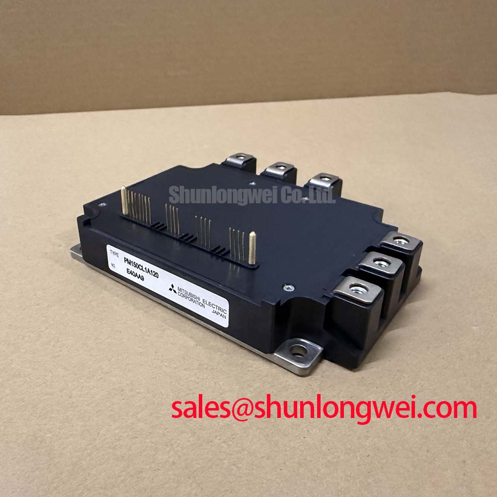
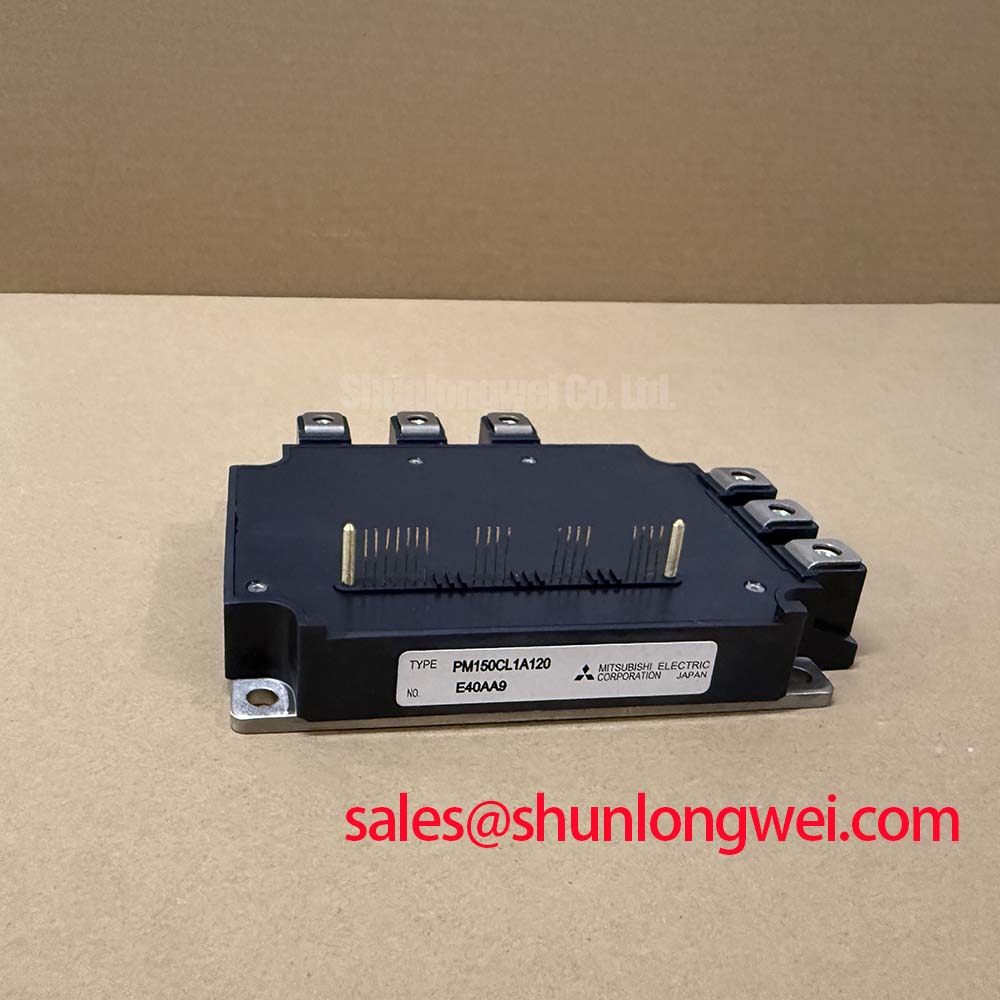
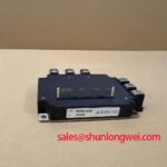
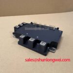
Before reconnecting a removed power stage, compare the nameplate boundary with the drive documentation and inspect the mounting face for residue, scratches, trapped particles, or uneven fastening marks. PM150CL1A120 is specified by Mitsubishi Electric as a 1200.0 V, 150.0 A Mitsubishi IGBT Module. Those official ratings identify the device category and electrical boundary, but they do not replace verification of the original inverter circuit, gate-drive arrangement, heat sink, protection path, and DC-link condition.
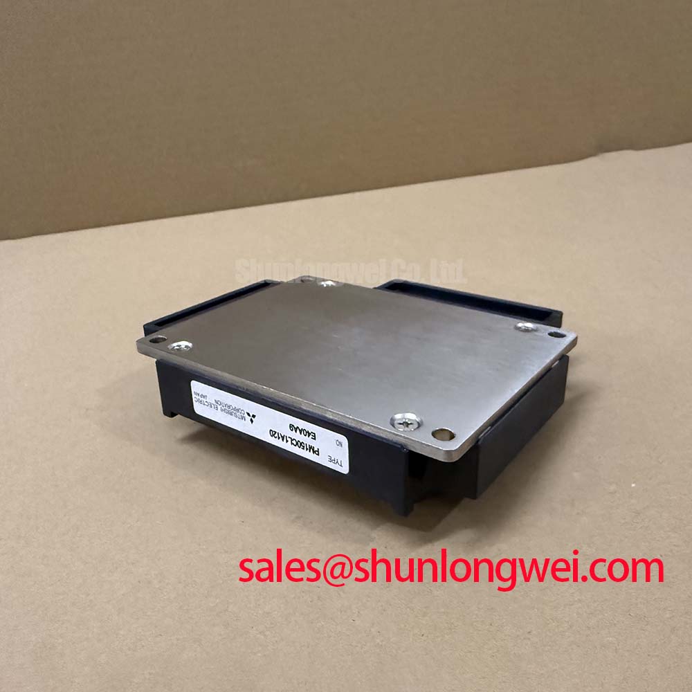
Thermal interface preparation is a practical first check when a power assembly has shown intermittent trips after service. A thin, continuous thermal interface material layer is generally used to fill microscopic mating irregularities between the module base and heat sink. As a Design Consideration, many service procedures target a controlled layer in the 50 to 100 um range where the material supplier, mounting surfaces, and original equipment instructions support that process. Excess material can add thermal resistance, while dry areas, debris, or local voids can create concentrated heating during load cycles.
Inspect the heat-sink plane with a straightedge and inspect the module underside before applying fresh material. A heat sink with local distortion can prevent uniform contact even when the interface layer initially looks satisfactory. The system engineer should assess whether the original mounting surface, retention method, and mechanical stack remain suitable rather than attempting to compensate for an uneven surface with a thicker paste layer.
Install the mounting hardware progressively in a cross-pattern sequence so clamping force develops evenly across the module. The final torque must follow the original equipment documentation and the applicable fastener specification; it is not an official PM150CL1A120 torque rating unless confirmed in the relevant Mitsubishi Electric documentation. After fastening, examine whether material has displaced uniformly at the perimeter without contaminating terminals, nearby insulation, or signal connections.
Field Alert: Isolate and discharge the DC link before loosening power terminals or mounting hardware, because stored energy and unintended conductor movement can damage the assembly or create a hazardous condition.
If a repaired inverter develops a fault only after warming under controlled load, avoid assigning the condition to the module from temperature alone. Record heat-sink temperature, enclosure airflow condition, switching activity, current feedback, and protection events. Uneven thermal transfer is one possible contributor, while a deteriorated fan, blocked airflow path, loose bus connection, control-board issue, or changing load can present similar symptoms. Mitsubishi Electric's power semiconductor and high-power module information provides useful manufacturer context when confirming the correct documentation family.
Benchtop Waveform Tuning: Mitigating Stress via Optocoupler vs Digital Coreless Transformer on PM150CL1A120
During a controlled bench investigation, first verify that every gate-drive command is absent before the DC link is energized, then compare the affected channel against a known-good channel using properly rated differential measurement equipment. The PM150CL1A120 is an IGBT module, so its specified 1200.0 V and 150.0 A ratings must be read alongside the original equipment schematic and approved application documentation. Do not infer the internal control interface, gate threshold, isolation rating, protection function, or recommended drive voltage from the module category alone.
Optocoupler-based and digital isolated-driver arrangements manage the same essential problem through different implementations: a switching power stage can create rapid common-mode voltage movement while the controller still needs an unambiguous command reference. Isolation barrier capability, common-mode transient immunity, supply sequencing, output state during startup, and fault-return behavior must be confirmed against the actual driver data sheet. Requirements such as reinforced isolation above a stated voltage or immunity above a stated transient rate are system-level requirements, not official PM150CL1A120 specifications unless Mitsubishi Electric explicitly states them for the installed assembly.
A Design Consideration is to keep the command return path coherent with the driver architecture and to separate sensitive control routing from high-current commutation paths. This reduces opportunities for switching current to couple into control wiring. When a false trip or unexplained transition is suspected, capture the command input, isolated output, local driver supply, fault indication, phase node, and DC-link behavior during the same event. A waveform anomaly may indicate an impedance, grounding, supply-decoupling, layout, or control-timing issue, but it should be compared with the known-good signal path before any part is assigned as the cause.
Interface-layer quality also matters during waveform work because repeated tests can heat the module and change observed behavior. For a service rebuild, a 50 to 80 um thermal-interface target can be a Typical Starting Point only when supported by the interface material manufacturer and original mechanical design. Use the established cross-pattern mounting sequence and approved torque for the hardware. Do not alter gate resistance, isolation components, or bootstrap networks based on a single overshoot image; component selection depends on the installed driver, switching frequency, topology, load, protective thresholds, and measured margins.
Bootstrap capacitor charging and diode recovery deserve inspection where a high-side driver supply is involved, but neither can be presumed to exist within this specific module without the original circuit information. Check the high-side supply waveform through the operating sequence, including start, load transition, and controlled shutdown. A low or unstable supply can affect command integrity, while the underlying reason may be charging-path resistance, diode behavior, decoupling condition, supply layout, or control logic. The system integrator should verify the required supply voltage and timing from the original inverter documentation.
For a neutral same-class reference during a compatibility review, engineers can compare documented voltage class, current requirement, circuit configuration, package outline, terminal layout, driver architecture, and protection behavior against the SKIIP37AC12T4V1. A matching headline voltage rating alone does not establish a direct replacement relationship.
PM150CL1A120 Operational Boundaries: Evaluating Thermal Stress Alleviation in Bidirectional Limits
For a commercial string inverter or micro-grid energy-storage converter evaluation, begin by confirming whether the installed topology actually permits bidirectional power transfer between battery racks and the inverter DC link. The presence of energy storage does not by itself define the switching arrangement, current path, regenerative operating mode, or control permissions. The official data available here identifies PM150CL1A120 as a 1200.0 V, 150.0 A Mitsubishi Electric IGBT Module; it does not establish a specific battery voltage, C-rate, switching frequency, overload capability, or thermal-cycle life.
During peak shaving, charging, discharge, or regenerative transitions, power devices can experience changing conduction and switching losses. The operational impact depends on duty cycle, phase current, DC-link voltage, heat-sink performance, ambient condition, modulation method, and the controller's transition strategy. A Design Consideration is to use the original system telemetry and controlled measurements to compare current, temperature, and fault behavior through both directions of expected power flow. This approach gives a more defensible service record than assigning a fixed allowable operating profile without the complete inverter design.
Where a drive includes regenerative braking, the braking chopper and braking resistor path require their own inspection. A resistor intended to absorb excess DC-link energy is part of the system protection strategy, not an attribute established by the PM150CL1A120 rating. Check the resistor connection, thermal condition, chopper control signal, DC-link measurement path, and event history against the equipment service information. A rising DC-link event may arise from a control-state issue, an energy-absorption path issue, abnormal regeneration, measurement error, or another system condition.
Repeated temperature movement can also reveal mechanical weaknesses around terminals and the heat-transfer stack, but no life duration or failure-rate prediction should be assigned without applicable manufacturer qualification information or a validated test source. Inspect fastener retention, busbar seating, heat-sink contact, cooling-system behavior, and connector condition. When integrating or servicing the unit, designers should verify that measured thermal and electrical conditions stay within the original equipment limits over the real operating sequence.
The relationship between switching behavior, losses, package constraints, and system efficiency is broader than any single power module page. For background that can support a separate engineering review, see Unlocking Efficiency in Industrial Drives. That resource is contextual material and does not modify the official specifications of PM150CL1A120.
Where the converter resumes operation after a repair, return it to service through the equipment maker's approved commissioning sequence. Observe protection indications and measurements during a controlled ramp rather than applying an unverified full-load command. This helps distinguish a resolved mechanical or connection issue from a condition that requires wider controller, sensor, or power-stage investigation.
Assembly Integrity & Layout Architecture: Implementing Turn-Off di/dt Induced Vpeak Clamping for PM150CL1A120
Inspect the DC-link busbar, capacitor connections, phase conductors, and power-terminal seating before attempting to interpret turn-off stress. At turn-off, the observed voltage at a switching device is influenced by DC-link voltage and by the voltage created as stray inductance reacts to changing current. In engineering terms, the peak includes the DC-link contribution plus an inductive term related to loop inductance and current-change rate. This is an Engineering Calculation principle, not a complete PM150CL1A120 operating limit, because accurate assessment depends on the actual commutation loop and valid high-voltage measurement practice.
As a Design Consideration, minimize parasitic loop inductance in the DC-link commutation path to suppress turn-off inductive overshoot. A compact, symmetrical planar busbar arrangement can help when it matches the equipment's insulation, creepage, clearance, assembly, and service requirements. The required spacing and layout cannot be prescribed from the module's 1200.0 V rating alone; the system engineer must validate the complete assembly against applicable equipment requirements and measured switching peaks.
Snubber networks should be evaluated as part of the complete converter rather than sized by a generic rule. Their capacitor type, location, connection inductance, damping, dissipation, and interaction with the DC-link capacitors determine whether they address the observed waveform without creating another problem. When a bench capture shows high-frequency ringing, first verify probe bandwidth, reference method, connection geometry, and repeatability. Then correlate the event with load current, DC-link condition, gate command, and protection response. A waveform that appears excessive may reflect the power loop, measurement setup, gate-drive behavior, capacitor path, or a combination of those factors.
Power and control layout should also preserve a clear separation between high-current paths and low-level sensing paths. Route current-feedback, voltage-feedback, fault, and command conductors according to the original design intent, with their reference returns understood. Loose terminal hardware or an altered busbar stack can change both electrical behavior and heat distribution. After reassembly, verify continuity where appropriate, confirm no unintended short exists between accessible conductors, and inspect the power stage under controlled conditions using procedures suitable for the equipment voltage and stored-energy hazard.
Mitsubishi Electric's global semiconductor device technologies information is an appropriate manufacturer reference point for broader device-family context. For PM150CL1A120 integration, the decisive evidence remains the correct model documentation, the original converter schematic, physical fit, and measured behavior in the intended system.