



Content last revised on October 28, 2026
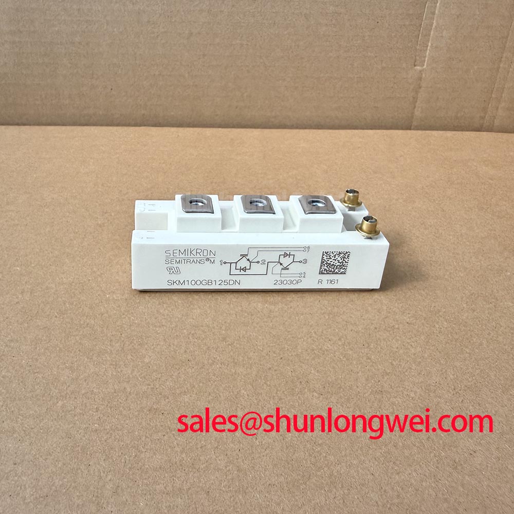
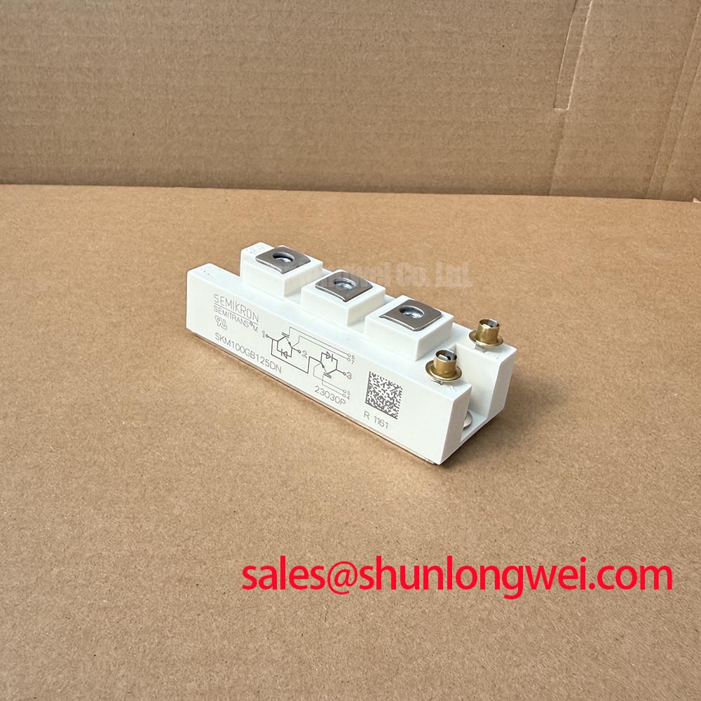
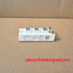
SKM100GB125DN Semikron 1200V 100A Semitrans IGBT Module
With the DC link fully discharged, check the module markings, terminal identification, and cold-state diode behavior before connecting a replacement to a traction inverter. The SKM100GB125DN is a Semikron IGBT module rated at 1200 V and 100 A, using the Semitrans package designation. These ratings identify the product class; current-rating conditions, switching current, pulse capability, thermal impedance, gate limits, and isolation test conditions must be taken from the applicable technical documentation used for the installation.
For incoming inspection, keep the power terminals isolated from the gate circuit and use an ESD-controlled bench. Confirm the printed polarity against the equipment schematic rather than relying on terminal position alone. A diode-range check can help establish a cold-state reference across the expected antiparallel diode paths, but the reading is only meaningful when compared with a known-good unit tested with the same meter leads, polarity, and temperature. A low-resistance reading between unrelated terminals or a result that changes materially with mechanical pressure deserves further investigation before energization. An isolated gate can retain charge and alter collector-emitter readings, so follow the manufacturer's gate-emitter handling procedure before interpreting those readings.
The module is relevant to engineers evaluating replacement power stages in industrial motor drives, including electric material handling and forklift traction systems. In these applications, the braking path, DC-link protection, cable arrangement, and gate-driver behavior determine whether the module operates inside a safe switching and thermal window. The 1200 V voltage rating and 100 A current rating identify the component class; they do not by themselves define the permissible duty cycle of a complete inverter.
SKM100GB125DN Operational Boundaries: Evaluating Thermal Cycling Margins in Braking Applications
Braking evaluation should begin at the energy path rather than at the nominal current label. During deceleration, the motor can return energy to the DC link faster than the battery interface or front-end converter can absorb it. In systems using a resistor braking chopper, the braking IGBT works with the braking resistor and its thermal mass to control link voltage. This is an application arrangement, not a claim that the module includes a dedicated braking circuit. The service engineer should record the DC-link voltage, braking command, pulse duration, repetition pattern, and heatsink temperature while the vehicle or machine performs its actual deceleration profile.
The 1200 V rating is a voltage specification for the device. The design team must still compare the measured switching peak and regenerative rise against the complete system boundary, including commutation overshoot and measurement tolerance. The 100 A rating is likewise a current specification under the applicable datasheet conditions, not a universal continuous braking-current allowance. Conduction loss, pulse duration, case temperature, cooling path, duty repetition, and the selected gate-drive conditions all influence the usable operating point.
For a braking chopper, size the resistor and switching interval from the kinetic energy that must be dissipated, then verify the result through temperature measurements and controlled transient testing. The resistor should not be treated as an isolated accessory. Its pulse rating, thermal recovery, wiring inductance, and enclosure heat transfer affect the voltage seen by the IGBT. A resistor that survives one long deceleration does not establish that the IGBT can tolerate the junction cycling caused by frequently repeated short braking events.
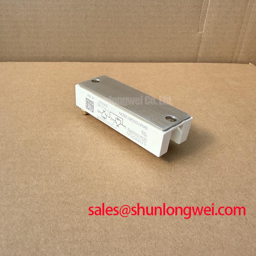
Thermal cycling margins are best assessed with the real mounting arrangement in place. Inspect the baseplate seating, thermal interface condition, heatsink flatness, airflow path, and fastener loading before comparing temperatures between the original and replacement device. If the case temperature rises unexpectedly while the electrical waveform remains similar, examine the mechanical heat path and thermal compound distribution rather than assuming an immediate semiconductor failure.
For cross-reference work, SK30GD123D may be reviewed as a separate Semikron part for an engineering comparison, but its electrical topology, terminal arrangement, ratings, and thermal data must be matched independently. A different current or voltage label is not sufficient evidence of interchangeability.
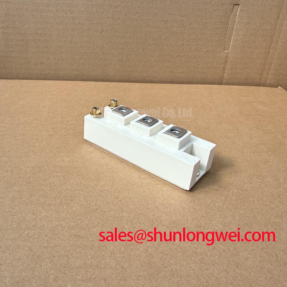
Semitrans packaging is part of the product identification supplied for this device. Mechanical fit, terminal spacing, baseplate dimensions, mounting provisions, and cooling requirements should be checked against the original assembly drawing before installation. The Semikron-Danfoss SEMITRANS® power module reference provides useful manufacturer-level context for the package family, while the individual part documentation controls the final connection decision.
| Item | SKM100GB125DN | Replacement comparison requirement |
|---|---|---|
| Manufacturer | Semikron | Confirm manufacturer and exact ordering code |
| Product category | IGBT module | Match topology and terminal function |
| Voltage rating | 1200 V | Compare official voltage and transient conditions |
| Current rating | 100 A under the applicable datasheet conditions | Compare conduction, pulse, and thermal conditions |
| Package designation | Semitrans | Verify mechanical and cooling compatibility |
Field Diagnostics and Commissioning: Terminal-to-Baseplate Insulation Checks
Isolation testing should be performed only after the gate driver, snubber, sensing harness, and other parallel circuits have been disconnected from the module. Use only the insulation-resistance or dielectric-withstand procedure authorized for the module and equipment; these tests are not interchangeable. The engineer must confirm that the test voltage, duration, terminal grouping, discharge method, and acceptance value are authorized by the applicable module documentation and equipment procedure.
Connect the insulation tester to the terminal grouping and baseplate specified by the authorized procedure, keeping personnel clear of exposed conductors. Do not apply the insulation-test voltage across semiconductor terminals or leave gate terminals in an unspecified state. Apply the test in a controlled sequence and discharge the module after the test. Record the ambient humidity and the condition of the heatsink area because airborne dust, moisture films, conductive residue, and contaminated thermal interface material can reduce the measured value without proving an internal semiconductor defect.
When the reading is below the site threshold, divide the circuit into smaller sections. Test the isolated module, then test the cable harness, snubber network, braking resistor connection, and heatsink assembly separately using procedures appropriate to each assembly. This approach distinguishes a module-to-baseplate insulation concern from a parallel path elsewhere in the power stage. Do not apply a megohmmeter to a connected gate driver, control board, current sensor, or communication interface unless that equipment is specifically rated for the test.
Gate-drive commissioning requires a separate low-voltage verification stage. Confirm the driver source and sink paths, gate-emitter reference, dead-time behavior, interlock operation, and fault response before applying the full DC link. The gate loop should have a deliberate return path and should not share a long, high-current emitter route with sensitive driver reference wiring. External gate resistance is a tuning element: its final value depends on gate charge, driver capability, switching speed, stray inductance, temperature, and the measured ringing waveform.
Use a suitably rated differential or isolated oscilloscope probe arrangement that does not create a long measurement loop or connect an earth-referenced ground lead to a switching node. Observe the gate-emitter waveform during controlled switching and look for overshoot, undershoot, ringing, or unequal turn-on and turn-off behavior. If adding damping reduces ringing but creates excessive switching loss, the correction may require a shorter loop, improved driver placement, or a different source and sink impedance rather than simply increasing resistance.
💡 Bench Tip: Preserve ESD protection and record a cold-state reference from a known-good module before interpreting diode-range or insulation readings.
Transient Dynamics and Electrical Design: Preventing High di/dt Gate-Loop Induced Triggering
High di/dt events can place a transient voltage across shared emitter inductance and disturb the gate-driver reference. Start by identifying the main load emitter connection and any separately marked auxiliary or Kelvin emitter return in the module documentation. Do not assume that two visually similar terminals have the same electrical role. The power return carries switching current; a dedicated auxiliary return, when provided for the applicable topology, should serve the driver reference and remain outside the high-current commutation path.
Trace the gate loop physically from the driver output to the gate terminal and back to its intended emitter reference. Keep the outgoing and returning conductors close together, minimize the enclosed loop area, and separate the control route from the collector or load-current path. The final clearance and conductor geometry are system design decisions governed by insulation requirements, switching voltage, enclosure construction, and measured transient performance.
A false gate event can appear as an unexpected pulse, irregular switching edge, or intermittent protection trip. These symptoms can also result from driver power instability, incorrect dead time, probe coupling, a damaged gate-emitter path, or an external control fault. Compare the gate waveform directly at the module terminals with the driver-side waveform while monitoring the collector-emitter transition. A difference between those locations points the investigation toward the interconnect and return path rather than allowing a single-cause diagnosis.
Long motor cables introduce another transient concern. Fast voltage edges traveling along the cable can reflect at impedance discontinuities, producing motor-terminal peaks higher than the steady DC-link value and reflections that travel back toward the inverter. The appropriate response may include a cable-rated output filter, controlled switching speed, revised termination, or a different motor-drive layout. The filter selection must follow the motor insulation rating, cable length, switching frequency, common-mode behavior, and measured waveform; no universal filter value should be assigned to this module alone.
During a controlled test, use differential voltage probes with suitable voltage ratings, bandwidth, and common-mode capability. Place the measurement point close to the module terminals and compare it with the motor-side waveform when investigating cable reflection. Check whether the peak is synchronized with a switching edge, a braking transition, or a commutation event. This timing information helps separate gate-loop disturbance from power-loop overshoot and prevents unnecessary changes to the control board.
Application reviews involving demanding traction or regenerative systems can also consult the Industrial Applications reference for broader power-electronics testing context. The Semikron-Danfoss power electronics hub supplies manufacturer-level reference material, while the actual terminal connection and operating limits remain specific to the applicable product documentation and system test results.
Preventing Spurious Faults: Transient Thermal Impedance Guidelines for SKM100GB125DN
Peak junction temperature during pulsed overload must be evaluated from the complete thermal path, not from heatsink temperature alone. The calculation starts with the measured or estimated power pulse at the IGBT, the case temperature at the same time reference, and the junction-to-case transient thermal response supplied for the device. A multi-RC thermal model can represent the short-pulse response, but its coefficients must come from the applicable device data rather than from a generic model assigned to every Semitrans module.
For a braking pulse, capture the current and voltage at the module, determine the instantaneous semiconductor dissipation, and apply the transient thermal response over the pulse duration. For repeated pulses, include the thermal recovery between events. A short interval between braking commands can leave the junction hotter than the case measurement suggests, especially when the heatsink has not yet responded to the previous pulse.
Any documented surge-current capability must be treated as a defined test condition, not as a routine operating target. If an ITSM rating is listed for an antiparallel diode, it must not be applied to the IGBT. A surge rating may depend on initial junction temperature, pulse width, circuit impedance, repetition, and the permitted recovery state. Before using any surge figure in a service decision, match the test conditions to the actual fault or braking event and confirm the value in the relevant Semikron documentation. The 100 A rating supplied for this product does not substitute for verified pulse-current or safe-operating-area data.
Semiconductor fuse coordination should be based on the available fault current, clearing time, fuse characteristic, wiring inductance, and any I²t withstand information documented for the relevant device element. A diode I²t rating does not establish IGBT short-circuit withstand capability. A fast fuse can limit fault energy, but it cannot correct an unsuitable gate command, inadequate dead time, excessive commutation inductance, or a short circuit located outside the protected branch. Fuse protection alone should not be assumed to protect an IGBT during a short circuit; fast electronic fault detection and controlled turn-off must be coordinated with the module’s documented limits.
When a drive reports an intermittent overcurrent or thermal fault, capture the event instead of resetting immediately. Review the DC-link level, braking command, gate waveform, phase current, heatsink temperature, and fault timing together. A protection trip may be associated with a genuine overload, cable reflection, driver supply disturbance, current-sensor error, or thermal accumulation from repeated pulses. Correlating these signals provides a more reliable path to corrective action than replacing the module without preserving the evidence.
Final commissioning should include a gradual increase in DC-link voltage and load while monitoring the electrical and thermal response at the actual switching frequency. Verify that the baseplate remains evenly seated, that the cooling path is unobstructed, and that the braking resistor does not heat adjacent control wiring. Record the tested operating envelope for the equipment so future service personnel can compare a replacement module against the original installation conditions.