


Content last revised on September 10, 2026
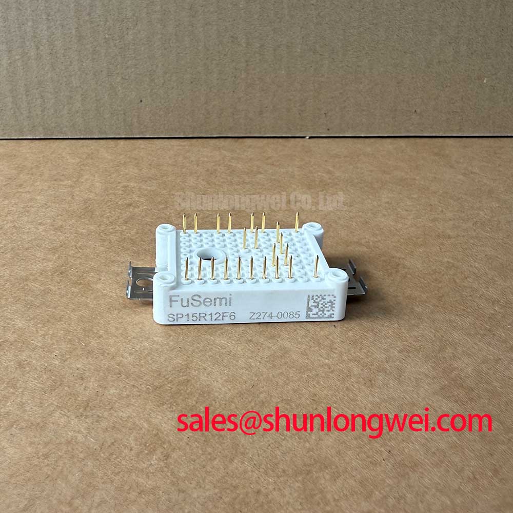
SP15R12F6 Circuit Protection and Reliability: Calibrating Heatsink Contact Pressure
| Parameter | Official Specification |
|---|---|
| Manufacturer | StarPower |
| Product category | IGBT Module |
| Collector emitter voltage | VCES = 1200 V |
| Continuous collector current | IC nom = 15 A at TC = 100°C |
| Repetitive peak collector current | ICRM = 30 A for tP = 1 ms |
| Total power dissipation | Ptot = 130 W at TC = 25°C and Tvj = 175°C |
| IGBT saturation voltage | VCE(sat) = 2.40 V at Tvj = 25°C |
| Inverter diode reverse voltage | VRRM = 1200 V |
| Rectifier diode reverse voltage | VRRM = 1600 V |
| IGBT thermal resistance | Rth(j-c) = 1.05 K/W |
Measure the temperature rise at the module baseplate and inspect the mounting surface whenever an operating drive shows increasing collector current stress, uneven phase temperature, or repeated thermal alarms. A clean heatsink, a flat contact area, and consistent mechanical pressure are essential to using the SP15R12F6 within its stated thermal conditions.
The official specification gives a total power dissipation of 130 W at TC = 25°C and Tvj = 175°C, together with an IGBT junction to case thermal resistance of 1.05 K/W. These values describe defined test conditions rather than a guaranteed heat load in every variable frequency drive. Actual junction temperature depends on switching frequency, current waveform, duty cycle, heatsink impedance, airflow, interface material, and enclosure temperature.
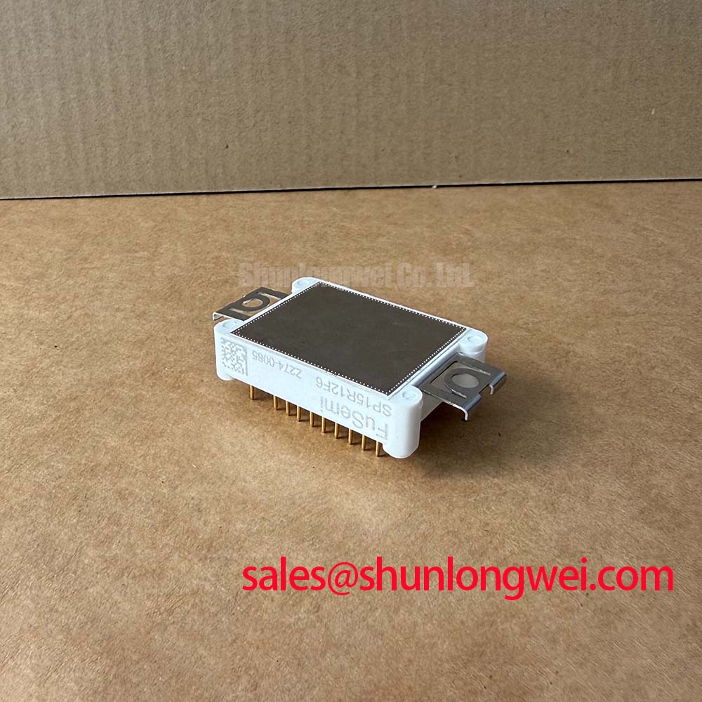
As a Design Consideration, remove the module and inspect the heatsink for burrs, contamination, local distortion, or a contact pattern that indicates uneven pressure. Apply the thermal interface material according to its supplier process. The target is continuous wetting of the mating surfaces with controlled thickness and minimal voids, not a thick layer intended to compensate for a curved baseplate. If curvature is present, correct the mechanical interface rather than forcing the module down with excessive local pressure.
Use a sequential tightening pattern so that pressure develops progressively across the module. The applicable torque must come from the original mechanical drawing, fastener specification, and heatsink design; it should not be inferred from the electrical ratings. Record the torque tool calibration status and inspect washers, threads, and mounting holes during preventive maintenance. A loose busbar connection can create localized heating that is easily mistaken for inadequate semiconductor cooling.
For pulse operation, review the manufacturer’s transient thermal impedance information rather than applying only the steady state thermal resistance. The pulse duration and repetition pattern determine how much heat remains in the junction when the next current event occurs. During commissioning, use thermocouples or an approved infrared method at accessible case locations and correlate the result with switching waveforms. A thermal model can then estimate peak junction temperature, but the model remains an Engineering Calculation that requires validation against measured operating conditions.
⚠️ Maintenance Note: Clean the heatsink and verify fan and airflow performance during scheduled service while monitoring contact temperature rise at comparable load points.
SP15R12F6 Thermal Electrical Optimization: Internal Braking and DC Link Energy
Trace the braking command, gate signal, DC link voltage, and braking resistor current together when a drive trips during deceleration. This separates a semiconductor switching problem from excessive regenerative energy, an open resistor path, a failed contactor, or an incorrect braking control sequence.
The SP15R12F6 provides a 1200 V collector emitter rating and a repetitive peak collector current rating of 30 A for a 1 ms pulse. Those are official device ratings, not a complete braking resistor design. The braking branch must be evaluated against the motor inertia, deceleration profile, DC link control threshold, resistor thermal capability, pulse duration, and permissible enclosure temperature. The ballast resistor absorbs kinetic energy as heat, so its short pulse rating and average power rating must both be assessed.
When checking a replacement assembly, identify every power terminal from the original circuit drawing and confirm polarity with an unpowered continuity inspection. Do not rely on physical position alone, because busbar arrangements can differ between drive revisions. Check creepage and clearance around the DC link, braking branch, and output conductors for contamination, loose hardware, or damaged insulation. These are Design Considerations for the complete assembly and are not additional factory specifications for this module.
Fast semiconductor fuses may be part of the protection strategy, but fuse selection requires coordination of prospective short circuit current, clearing time, semiconductor withstand capability, and the fuse’s published I2t characteristic. A fuse that survives normal acceleration can still provide inadequate protection during a low impedance switching fault. The final protection study should use the fuse manufacturer’s time current data and the drive manufacturer’s short circuit procedure.
Gate drive integrity deserves equal attention. Inspect the gate resistor, isolation device, return path, and connector for cracked solder joints or contamination. An optocoupler or digital isolator used in an industrial drive should be evaluated for its specified common mode transient immunity under the actual gate loop conditions. CMTI is a property of the selected isolation component and circuit implementation, not a rating that can be assigned to the SP15R12F6 itself.
For a neutral comparison during a repair assessment, engineers may also review the electrical and mechanical documentation for FZ800R12KS4_B2. Any substitution remains system dependent and requires verification of terminal arrangement, thermal interface, gate requirements, protection coordination, and control timing.
Assembly Integrity and Layout Architecture: Sinusoidal Filter or dv/dt Reactor
Capture the motor terminal waveform with a suitable differential probe when a heavy duty variable frequency AC motor drive reports insulation stress, audible motor noise, or unexplained overvoltage during long cable operation. Compare the waveform at the inverter output and at the motor terminals, because cable reflections can produce a materially different voltage pattern at the load.
The SP15R12F6 has a 1200 V VCES rating and an inverter diode reverse voltage rating of 1200 V. These ratings do not define the allowable voltage overshoot of a particular motor cable installation. Cable length, characteristic impedance, termination, switching edge rate, motor insulation, grounding, and layout parasitics all influence the terminal waveform. A long transmission path can reflect switching energy and create a peak approaching twice the local DC link voltage under unfavorable conditions, so the actual peak must be measured rather than assumed.
A dv/dt reactor reduces the steepness of the applied voltage transition and can be appropriate when the motor and cable system can tolerate the remaining waveform. A sinusoidal filter uses a more complete output filtering network to produce a waveform closer to a sine wave, but it introduces additional impedance, losses, resonance considerations, and control loop effects. The system designer should select the topology after reviewing motor insulation requirements, cable construction, switching frequency, drive current, and filter manufacturer data.
Keep the high current commutation loop compact and route gate control wiring away from the collector and DC link conductors. Minimize parasitic loop inductance to suppress turn off inductive overshoot, then verify peak voltage and current margins with an oscilloscope during the actual switching test. Do not assign a fixed clearance or inductance value without the enclosure geometry, insulation system, pollution environment, and applicable safety requirements.
Inspect busbar fastening after thermal cycling and vibration exposure. A joint with increasing resistance can generate heat and add stray inductance, while an inadequately supported conductor can transfer mechanical stress to the module terminals. When integrating the module into a replacement drive, compare the original busbar stackup, insulation barriers, snubber location, and filter connections. The related front end or auxiliary stage can be reviewed through SKM75GB07E3 as a separate topology reference, without treating it as an automatic substitute for the installed circuit.
The communication layer of a motion system does not remove the need for physical waveform verification. For equipment using coordinated motion control, the Sercos III real time communication interface may define timing between control nodes, but it does not establish the power module’s switching margins or motor cable compatibility.
Transient Dynamics and Electrical Design: Static and Dynamic Current Distribution
Probe the gate emitter command and collector emitter voltage on each paralleled switching path when current sharing appears uneven or one phase runs hotter than the others. Check the gate loop resistance, conductor length, return routing, and local auxiliary connections before attributing the imbalance to the semiconductor die.
The official VCE(sat) value is 2.40 V at Tvj = 25°C. IGBT saturation voltage generally changes with current and temperature, so the value should be used as a datasheet reference point rather than a constant operating drop. In steady state, the electrical characteristics can support a degree of static current balancing, but the complete result also depends on emitter resistance, busbar symmetry, thermal coupling, and the impedance of every parallel path.
Dynamic sharing is more sensitive to layout. Match the gate path geometry, keep the drive return paths controlled, and avoid routing one channel beside a high di/dt collector conductor while another channel follows a quieter path. Gate loop parasitic inductance can create ringing, delayed turn on, or unwanted turn off behavior. A damping network may be evaluated as a Typical Starting Point during bench tuning, but its final value must be selected from measured gate voltage, switching loss, and electromagnetic behavior.
Check the gate waveform under the intended DC link voltage and load current, not only with a low voltage functional test. Confirm that the isolation barrier remains stable during the highest common mode transition and that dead time prevents cross conduction in the complete bridge. If the waveform differs between channels, compare connector contact resistance, driver supply impedance, gate resistor population, and mechanical routing.
For difficult transient conditions, review switching overshoot, short circuit response, thermal impedance, and protection coordination together. The Wide Bandgap Revolution reference provides broader practical context for comparing fast switching technologies, but it does not replace the StarPower electrical ratings or the measured limits of this silicon IGBT installation.


