


Content last revised on September 20, 2026
Benchtop Waveform Tuning: I2t Coordination and Sub-Cycle Surge Evaluation for TD500N12KOF 5DN
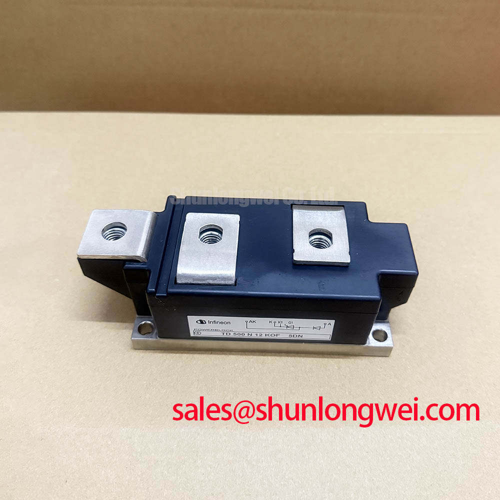
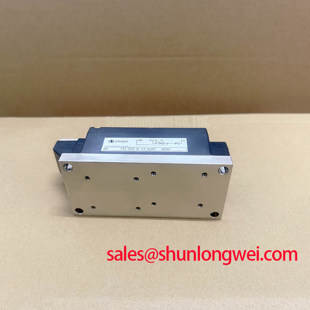
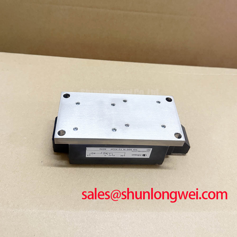
The TD500N12KOF 5DN is specified for 500 A average on state current at Ths = 85°C, 785 A RMS on state current, and a 12500 A surge current at 50 Hz for 10 ms. These are Official Datasheet Specifications and define distinct operating conditions. The 10 ms surge rating is a short duration withstand figure, not a continuous current allowance or a substitute for branch fault protection.
For a dead short evaluation, the protection engineer should obtain the semiconductor fuse manufacturer’s time current and pre arcing I2t information, then compare the fuse clearing behavior with the protected circuit’s fault path and the module’s stated surge capability. The supplied module data does not provide a published I2t withstand value, so an exact I2t coordination calculation cannot be represented as an official capability for this part. Verification should include the actual AC source impedance, transformer contribution, busbar impedance, fuse position, and the current waveform measured at the installed assembly.
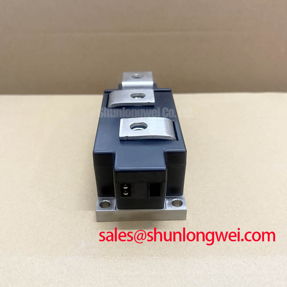
Terminal hardware should be tightened using the module documentation and the equipment maker’s approved fastening procedure. Uneven terminal contact or an uncontrolled torque sequence can add resistance, create localized heating, and complicate fault waveform interpretation. ⚡ Safety Interlock Note: Isolate and discharge the DC link before loosening any power terminal or measurement lead.
For repair planning, TD210N12 can be reviewed as a related replacement reference, but the system integrator should verify current rating, mechanical interface, firing circuit connection, thermal path, and protection coordination against the original assembly before installation.
TD500N12KOF 5DN Thermal Electrical Optimization: Gate Firing and Pulse Train Timing Practical Tuning
Gate firing behavior is determined by the thyristor section and the connected control board, while diode conduction is determined by circuit polarity and commutation conditions. The available official parameters for TD500N12KOF 5DN do not state gate trigger current, gate voltage, holding current, latching current, gate pulse rise time, or allowable gate pulse train characteristics. Those values should therefore be confirmed from the original equipment documentation or the complete manufacturer datasheet before any firing board adjustment.
As a Design Consideration, inspect the gate and auxiliary wiring as a separate low energy path from the high current power loop. Shared return paths, long control leads, and poor connector engagement can alter observed firing behavior or expose the control interface to switching noise. Engineers should capture gate to cathode behavior and the associated anode current waveform with correctly rated isolated instrumentation, comparing results with a known good channel where one is available.
Current rise and turn off stress are influenced by busbar geometry, source inductance, commutation components, and the selected protection network. Minimize parasitic loop inductance where high current transitions can produce voltage overshoot, then verify peak voltage margins against the DC link and the 1200 V official rating during controlled switching tests. The device’s specified maximum on state voltage is 1.65 V at ITM = 1500 A and Tj = 25°C; it is a defined test condition rather than a prediction of installed voltage drop under every thermal and conduction waveform.
💡 Pro Tip: Keep positive and return busbar paths physically symmetric around the commutation loop, then validate the resulting transient voltage with a properly referenced measurement setup.
For broader context on fault modes, current paths, and practical power semiconductor test methods, maintenance teams can use The Ultimate IGBT Knowledge Base as a technical reference while applying the specific TD500N12KOF 5DN ratings above.
Assembly Integrity & Layout Architecture: Mechanical Mounting and Thermal Management for TD500N12KOF 5DN
Thermal installation begins with a clean, flat heatsink interface and a controlled fastening sequence that progressively distributes clamping force across the module base. The official thermal resistance is 0.065 K/W junction to heatsink per module. This value supports thermal assessment only when the stated mounting boundary is reproduced; it should not be treated as a complete enclosure or coolant loop thermal model.
A thin, continuous thermal interface layer should be applied according to the approved assembly process, followed by diagonal and incremental tightening of the mounting fasteners. The manufacturer documentation must control the final torque because the supplied official parameters do not identify screw size, baseplate geometry, or a dedicated mounting torque value. After installation, inspect for rocking, uneven paste transfer, damaged threads, and busbar stress transferred into the power terminals.
When a high current green hydrogen electrolyzer DC power rectifier is being evaluated, the heatsink temperature measurement point should be correlated with the actual coolant or airflow condition. Designers should verify junction temperature margin from the full duty waveform, ambient condition, cooling performance, and rectifier loading profile rather than relying on average current alone. Infineon’s EconoPACK™ Plus module information can be useful for reviewing general module integration practices, while it does not replace the TD500N12KOF 5DN product documentation.
Assembly Integrity & Layout Architecture: Post-Surge Reverse-Voltage Inspection for TD500N12KOF 5DN
Following an abnormal half cycle event, do not reapply reverse voltage solely because the external fuse appears intact. The 12500 A, 50 Hz, 10 ms ITSM rating is an Official Datasheet Specification for a defined surge condition. Actual fault exposure can differ because current amplitude, waveform shape, initial junction temperature, series inductance, and fault duration are system determined.
A practical post surge inspection should begin with safe isolation, visual examination of terminals and mounting hardware, and controlled electrical checks against the equipment’s approved maintenance procedure. Where the rectifier can be tested safely, compare forward and reverse blocking behavior with a known good phase or a documented baseline. Unexpected readings may indicate a damaged module, a parallel path elsewhere in the assembly, or a measurement setup issue, so circuit isolation and repeatable instrumentation matter.
The module provides 3000 V RMS isolation voltage at 50 Hz for 1 minute as an Official Datasheet Specification. This rating should not be interpreted as a complete system insulation certification. Clearance, creepage, enclosure pollution level, cable routing, and test method remain responsibilities of the complete equipment design. For related low voltage power semiconductor technology context, see Infineon’s OptiMOS™ Low Voltage MOSFETs portfolio, which is technically distinct from this high current thyristor/diode module.