Content last revised on September 16, 2026
TT162N14KOF Operational Boundaries: Evaluating AC Line Surge Immunity and Lightning Transient Limits
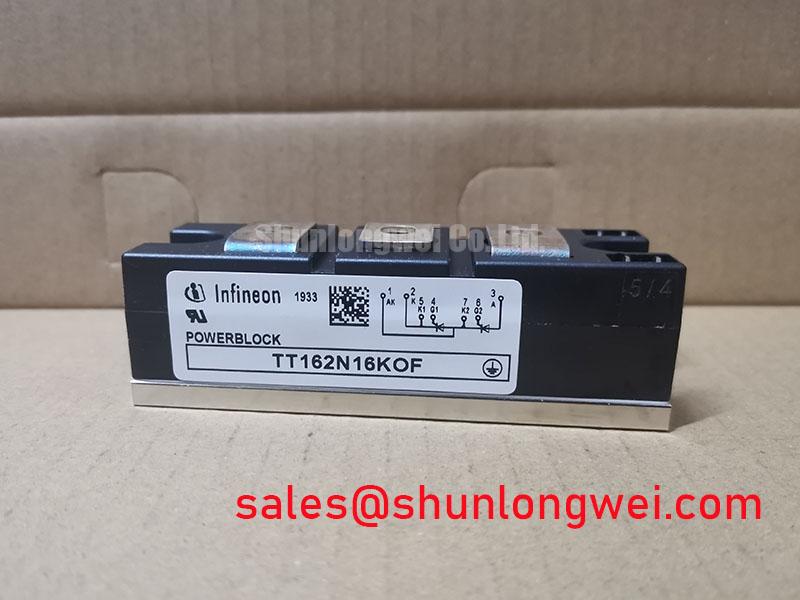
Before reconnecting a failed valve assembly, isolate the cabinet and verify the module marking against the original circuit position, then inspect the power terminals, insulator faces, and heatsink contact area for looseness, arcing traces, or distortion. The TT162N14KOF is an Infineon dual thyristor module with a 1400 V repetitive peak voltage rating and an 162 A average on-state current rating at Tc = 85°C, both specified device ratings.
The 1400 V VDRM and VRRM ratings define the repetitive blocking boundary of the device. They do not, by themselves, prove that an assembled grid-connected Static Var Compensator or thyristor-switched capacitor bank will withstand lightning-related line events. MOV selection, RC snubber design, incoming surge protection, busbar routing, and the measured clamping behavior of the complete installation remain design considerations. Engineers should validate surge performance against the applicable system standard, such as IEC 61000-4-5 where required by the equipment specification.
| Official Datasheet Specification | Rated Value | Integration Relevance |
|---|---|---|
| Repetitive peak voltage, VDRM / VRRM | 1400 V | Defines repetitive blocking-voltage capability. |
| Average on-state current, ITAVM | 162 A at Tc = 85°C | Defines continuous current capability under the stated case temperature. |
| Surge on-state current, ITSM | 5200 A | Relevant to short-duration fault and inrush coordination. |
| Critical rate of rise of voltage, dv/dt | 1000 V/µs | Indicates resistance to unintended triggering from fast voltage transients. |
| Maximum junction temperature, Tvj max | 125°C | Thermal operating limit for cooling-system verification. |
The specified 1000 V/µs critical dv/dt is particularly relevant when capacitor-bank switching creates steep recovery voltages. Snubber components should be assessed from measured waveform behavior at the thyristor terminals, including the influence of the return conductor and adjacent switching branches. For broader context on industrial power-device portfolios, consult Infineon High Power Semiconductor Solutions.
Transient Dynamics & Electrical Design: Fault-Current Coordination on TT162N14KOF
For a suspected dead-short event, check the upstream semiconductor fuse indication and examine both current paths before fitting a replacement module. The 5200 A ITSM value is a specified surge-current rating for the device, but it is not a substitute for coordinated fault clearing. A semiconductor fuse must interrupt the prospective fault before the current-time stress exceeds the device capability under the actual circuit conditions.
Fuse coordination is an Engineering Recommendation: compare the fuse pre-arcing and total-clearing I²t data with the thyristor module documentation, the available fault current, and the operating point of the SVC or capacitor-switching branch. The comparison must include the complete protection path, because cable impedance, transformer source impedance, parallel branches, and fuse mounting all influence clearing behavior. No universal fuse I²t value can be assigned to TT162N14KOF without those system measurements and the relevant manufacturer curves.
Terminal hardware deserves the same attention as the protection calculation. Clean contact faces, correct conductor seating, and mechanically secure connections reduce localized resistance that can complicate thermal diagnosis after a fault. ⚠️ Field Alert: Isolate and discharge the capacitor bank before touching module terminals, and apply the equipment manufacturer’s specified terminal and heatsink fastener torque.
Where a circuit review identifies substantially higher continuous-current demand, the TT570N16 can be evaluated as a separate module with its own voltage, current, mechanical, and gate-drive requirements; it should not be treated as a direct substitution without a full system check.
TT162N14KOF Operational Boundaries: Evaluating Baseplate Thermal Resistance Limits
After verifying that the module is electrically isolated, inspect the removed interface pattern on the heatsink. Uneven thermal-compound transfer, particles, scratches, or a bowed mounting surface can prevent uniform heat transfer even when the external cooling fan appears operational. The maximum specified junction temperature is 125°C, an Official Datasheet Specification. The 162 A at Tc = 85°C rating is therefore meaningful only when the installed cooling path maintains the stated case-temperature condition.
Thermal resistance from junction to case, heatsink flatness, compound specification, airflow, coolant performance, and mounting force must be verified from the original module documentation and equipment design. These factors are a Design Consideration, rather than published TT162N14KOF values in the supplied specification set. Engineers should compare temperature measurements across equivalent valve positions and investigate any abnormal difference before attributing a trip to the module alone.
For industrial display and control-panel reliability topics that may be relevant to the same cabinet environment, see The Ultimate Guide to Industrial TFT LCD Technology. Its display-integration guidance should be assessed separately from the thyristor thermal path.
Assembly Integrity & Layout Architecture: Implementing High-di/dt Gate Firing Pulse-Train Timing for TT162N14KOF
When one phase position fails to latch consistently, begin by comparing the gate-drive waveform and terminal routing with a known-good phase while the equipment is operated under controlled service procedures. Gate-circuit continuity alone does not confirm correct firing. Pulse width, pulse-train timing, gate-current rise behavior, holding-current conditions, and the voltage across the main terminals all affect whether a thyristor turns on uniformly.
Gate trigger current, gate trigger voltage, holding current, latching current, and permissible gate-pulse limits are not included in the supplied official parameter set. The system integrator should verify these values from the original TT162N14KOF documentation before changing gate resistors, isolation stages, or firing transformers. A multi-pulse firing approach can be evaluated where the control topology requires dependable turn-on through changing AC-line conditions, with final timing determined by system tests.
Keep gate and return paths compact to reduce coupled switching noise, especially where high current rises in neighboring branches can disturb the firing circuit. The module’s 1000 V/µs critical dv/dt rating helps define the device boundary, while actual immunity depends on the complete snubber, layout, and gate-driver arrangement. Infineon’s HybridPACK™ Drive information provides additional manufacturer context on power-module integration practices.