

Content last revised on September 10, 2026
Transient Dynamics and Electrical Design for 1MI100H-025
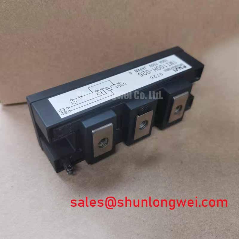
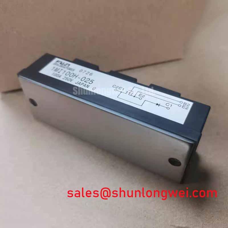
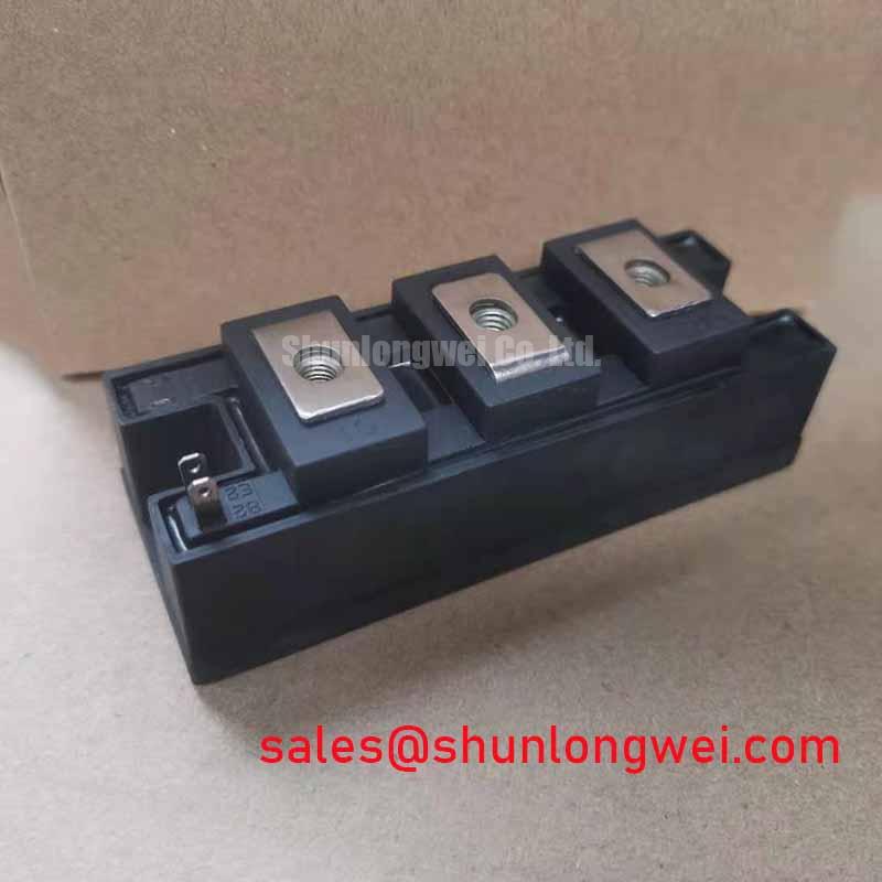
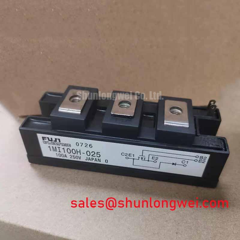
Begin the service check with the power removed: inspect the Fuji Power Module package for cracks, contamination, loose terminals, and heat-transfer marks, then verify the nameplate boundary of 1200.0 V rated voltage and 100.0 A rated current against the original inverter welder or induction-heating power stage. These values are official specification data supplied for 1MI100H-025; they are not a substitute for checking switching frequency, duty cycle, cooling conditions, or overload requirements in the equipment documentation.
The module is a Fuji Electric IGBT Module in a Fuji Power Module package. The product page does not establish a complete internal gate-drive circuit, isolation rating, common-mode transient immunity, thermal resistance, switching energy, or terminal arrangement. Before energizing a replacement, the system integrator should verify those parameters from the original equipment schematic and the applicable Fuji Electric documentation. Fuji Electric’s Power Semiconductor and IPM Modules resource provides the appropriate manufacturer context for this verification.
For an optocoupler driver, the engineering review should cover propagation-delay variation, isolation coordination, collector or output-stage behavior, and the possibility of a false gate signal during a high-voltage transition. A digital coreless transformer driver requires the same system-level attention, with additional checks for pulse transfer, reset behavior, and common-mode transient immunity. Do not assign a reinforced isolation or CMTI value to this module unless that value is confirmed for the selected gate-driver circuit and its isolation components.
Keep the gate-drive return path tightly associated with the corresponding emitter path, and separate power commutation current from control-signal routing. The useful field test is a differential probe comparison between the gate-to-emitter waveform and the local driver reference while the DC link is at the intended test condition. Unexpected gate movement should be investigated alongside driver supply stability, isolation-barrier behavior, probe-loop pickup, and commutation layout rather than attributed to the IGBT module alone.
When evaluating a related Fuji Electric part for mechanical or electrical compatibility, 3MBI50SX-120-02 may be reviewed as a separate reference model. It should not be treated as an automatic substitute because pin assignment, electrical ratings, thermal interface, and switching behavior must match the host equipment.
Benchtop Waveform Tuning and Turn-Off Overshoot Control
Use a controlled double-pulse or equivalent switching test to examine turn-on and turn-off behavior before connecting the module to the complete load. During turn-off, stray inductance in the commutation loop combines with current-change rate and can raise the collector-emitter voltage above the DC-link level. This relationship is an engineering calculation principle, not an additional factory rating for 1MI100H-025. The measured peak must be compared with the module’s verified voltage boundary under the actual operating temperature and current.
Busbar symmetry is especially important in an industrial inverter welder and in a medium-frequency induction-heating converter, where pulsed current can make layout asymmetry visible as ringing, overshoot, or uneven device stress. Minimize the physical area of the high-current commutation loop, keep the positive and negative conductors closely coupled, and place any snubber or clamp network according to the measured current path. Snubber capacitance and damping should be selected from oscilloscope results, switching energy, capacitor pulse capability, and acceptable loss. A nominal capacitor value cannot be prescribed without the complete topology and waveform data.
Gate interlock testing should confirm that the complementary devices cannot conduct simultaneously during command transitions, reset events, or loss of one driver supply. Dead time is a system-determined timing margin. Designers should establish it from measured propagation delay, temperature variation, gate-charge behavior, driver asymmetry, and the required output waveform, then verify that excessive dead time does not create unacceptable diode conduction or recovery stress.
Freewheel diode reverse-recovery softness is also relevant to EMI and voltage overshoot. The recovery waveform should be observed at the actual current and temperature rather than reduced to a single soft-factor assumption. A sharper recovery event can increase commutation disturbance, but the resulting behavior depends on the diode technology, bus inductance, gate resistance, load power factor, and switching conditions. Use the waveform to guide damping and layout changes.
💡 Pro Tip: Disconnect the DC link and confirm the discharge state before removing gate-drive or power terminals, because residual energy can damage the module and test equipment.
Assembly Integrity and Output Filter Architecture
Mechanical installation begins with a clean, flat heatsink surface and a verified interface material suitable for the assembly. The module mounting method, terminal hardware, insulation arrangement, and tightening procedure should follow the original Fuji Electric mechanical documentation. Do not infer a mounting torque, baseplate flatness tolerance, or creepage requirement from the model number alone.
In a long-motor-lead inverter system, cable impedance and propagation effects can produce terminal ringing and reflected voltage. A measured terminal spike approaching twice the local DC-link step is a design consideration for long interconnects, not a guaranteed behavior of this model. Check the waveform directly at the module output and at the motor terminals with suitable differential measurement equipment. The comparison can reveal whether the dominant issue is cable reflection, common-mode current, switching edge rate, grounding arrangement, or output-filter interaction.
A sinusoidal filter and a dv/dt reactor serve different system objectives. A sinusoidal filter targets a more complete reconstruction of the motor waveform, while a dv/dt reactor limits edge stress and can reduce cable-related disturbance without providing the same waveform transformation. Filter selection must account for switching frequency, motor insulation limits, cable length, load current, resonance, thermal loss, and control-loop interaction. The system integrator should verify the manufacturer’s filter data rather than treating either topology as universally suitable.
The upstream power path also matters during fault analysis. The 6MBI300U-120 can be examined as a separate rectifier or complementary-stage reference in a broader converter architecture. It does not define the input topology or protection requirements of the 1MI100H-025 application. Measure DC-link ripple, rectifier commutation, precharge operation, and fault-clearing response as part of the complete equipment review.
For parallel-device arrangements, positive temperature coefficient behavior may support static current sharing, but dynamic sharing remains dependent on gate-loop impedance, emitter routing, driver matching, thermal coupling, and switching timing. Engineers should confirm current balance with current probes during turn-on and turn-off. A module rated at 100.0 A should not be interpreted as a blanket permission to parallel units or operate at that current under every pulse width, cooling condition, or switching frequency.
Operational Boundaries and Transient Thermal Evaluation
Thermal verification should start with the actual duty cycle rather than a nameplate-only calculation. The official data available for this product identifies 1200.0 V, 100.0 A, and the Fuji Power Module package, but it does not establish a complete transient thermal impedance curve in the supplied parameter set. Junction temperature therefore requires confirmation from the applicable manufacturer datasheet, measured case temperature, device losses, heatsink behavior, and the real pulse sequence.
For a pulsed overload, a multi-RC thermal model can represent the changing junction-to-case response more realistically than a single steady-state resistance. The calculation should combine conduction loss, switching loss, pulse duration, repetition pattern, case temperature, and the thermal path to the heatsink. This is an engineering calculation and must be checked against the official thermal impedance data for the exact module revision. If that curve is unavailable, use conservative bench testing and temperature instrumentation rather than inventing a transient thermal constant.
During a fault investigation, record collector-emitter voltage, current, gate-to-emitter voltage, case temperature, DC-link behavior, and protection timing in the same test condition. A failed module may reflect excessive overshoot, inadequate gate control, cooling degradation, load short circuit, diode recovery stress, or an upstream protection problem. The measurement sequence should compare the affected phase with a known-good phase and should preserve the original wiring arrangement before component substitution.
Gate-trigger discussions involving a separate thyristor stage should remain distinct from the IGBT gate-drive analysis. Thyristor parameters such as gate trigger current and gate trigger voltage belong to the thyristor control circuit; they do not describe the gate requirements of this Fuji Electric IGBT module. Where a converter combines both technologies, verify each device family against its own documentation and examine pulse-train timing, isolation, and fault coordination at the system level.
For broader technology context when comparing silicon IGBT switching stages with other 1200 V conversion approaches, see The 1200 V CoolSiC™ MOSFET Advantage in Three. That material is a separate technical reference and does not alter the official ratings or compatibility requirements of 1MI100H-025. Procurement and repair teams should match the replacement against the original electrical ratings, package, terminals, driver interface, cooling method, and verified switching test results.