

Content last revised on September 21, 2026
CM400DY-12H Evaluation Overview
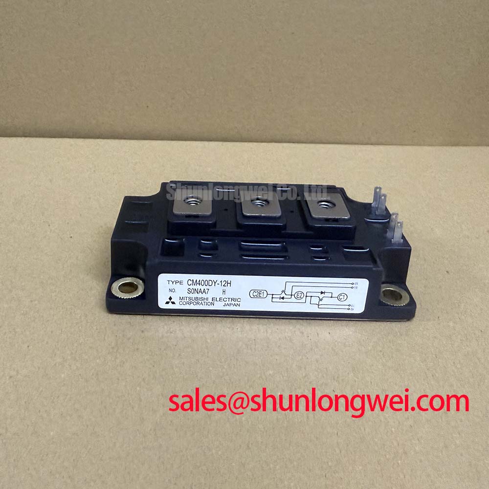
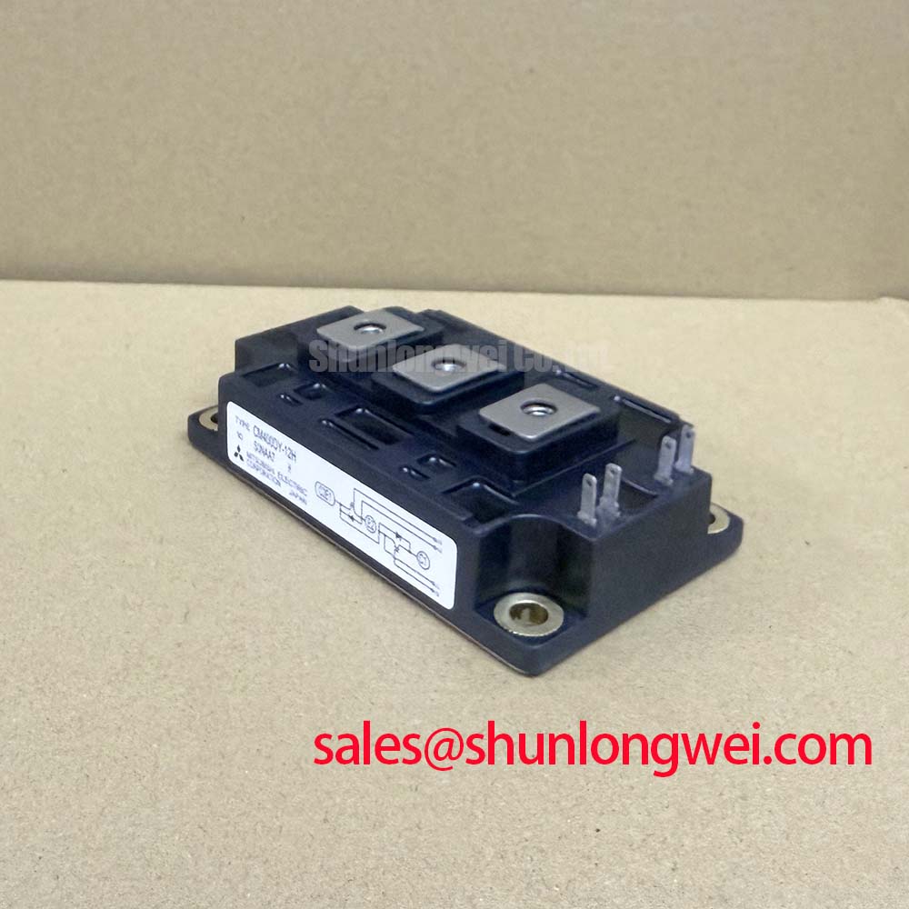
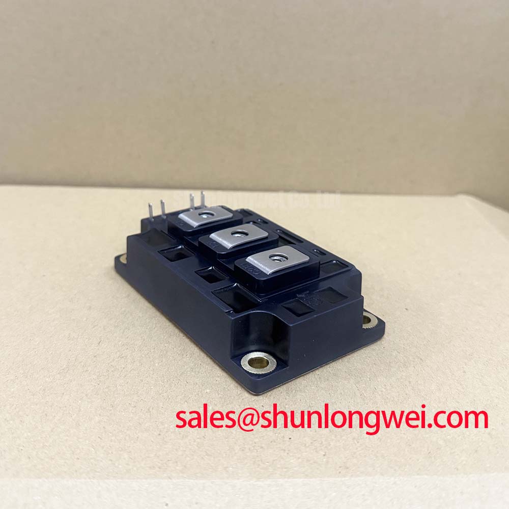
With the converter isolated and discharged, first verify that the cabinet documentation calls for CM400DY-12H, then inspect the module terminals, mounting face, and connected buswork before any powered test. This Mitsubishi Electric power semiconductor is a 600 V, 400 A IGBT module, based on the official supplied rating information. Confirm that these electrical limits match the original inverter position and DC bus architecture; a matching housing category alone does not establish electrical interchangeability.
| Parameter | Value | Classification |
|---|---|---|
| Manufacturer | Mitsubishi Electric | Product identification |
| Part number | CM400DY-12H | Product identification |
| Rated voltage | 600 V | Official Specification |
| Rated current | 400 A | Official Specification |
| Package | Module | Official Specification |
For repair evaluation in a utility-scale centralized battery energy storage PCS, document the bus voltage, switching topology, driver board arrangement, cooling path, and protection response before deciding whether this module is appropriate for the original location. The rating label defines key device boundaries, while actual switching stress remains dependent on the complete power stage, including conductor inductance, commutation path, gate drive behavior, thermal interface condition, and control protection timing.
Transient Dynamics & Electrical Design: Voltage Derating Considerations for CM400DY-12H
Check the measured DC bus voltage and recorded transient waveform against the 600 V official voltage rating before returning a CM400DY-12H installation to service. Voltage excursions at turn off are shaped by the total commutation loop, including laminated busbar condition, capacitor placement, terminal contact quality, and the current interruption rate commanded by the gate driver. A controller fault record that reports overvoltage is useful evidence, but it should be correlated with a suitably rated differential measurement at the power stage rather than treated as proof of one failed part.
Cosmic ray and terrestrial neutron exposure are high-risk reliability subjects. No official FIT rate, single-event burnout qualification result, altitude derating curve, or voltage-dependent failure model has been supplied for this specific module. A numerical SEB prediction or a mandatory altitude operating limit would therefore be unsupported. As a Design Consideration, system engineers evaluating high-elevation PCS installations should establish their own DC bus operating envelope from the complete equipment qualification plan, environmental location data, switching waveform measurements, and applicable system requirements.
In field troubleshooting, inspect for evidence of busbar displacement, loose DC link capacitor connections, contamination across high-voltage clearances, or an altered snubber arrangement after a maintenance event. These conditions can change the transient environment without changing the programmed bus voltage. Keep high-current commutation conductors physically compact to suppress turn-off inductive overshoot, then verify peak device voltage under the actual switching conditions. Mitsubishi Electric’s power semiconductor portfolio information is a useful manufacturer reference when matching a power device family to the wider converter design context.
When a lower-current member of the same general voltage class is being reviewed for a separate cabinet position, CM100DY-12E can be examined as a comparison point. Its part number must not be treated as a direct substitute for a 400 A module. The system integrator should compare current capability, package interface, driver compatibility, thermal path, protection settings, and original equipment documentation before any replacement decision.
CM400DY-12H Thermal-Electrical Optimization: Negative Gate Bias and Active Miller Clamp Practical Tuning
Before changing gate drive hardware, capture the gate-to-emitter waveform at the module connection reference used by the existing driver design. During hard commutation, a changing collector voltage can couple through the device capacitances and raise gate potential on the non-commanded switch. The result may be ringing, irregular current sharing in paralleled paths, or a protection event that appears intermittent. These symptoms require waveform correlation with collector voltage and phase current because they can also arise from return path coupling or a deteriorated driver supply.
Negative off-state gate bias and an active Miller clamp are driver-level measures that designers may evaluate to hold an off-state gate more securely during high-voltage transitions. The required bias value, clamp threshold, drive source and sink capability, isolation rating, and gate resistance cannot be assigned from the available CM400DY-12H official ratings. They must be selected and validated by the system designer against the original driver circuit and switching tests. A low-impedance active clamp path is relevant only when its layout reference remains controlled at the module and its operation is confirmed across the equipment’s real operating range.
Gate resistance is a tuning element rather than an arbitrary service part. Increasing damping can reduce ringing but may change switching loss and fault response. Reducing damping can accelerate transitions while raising sensitivity to stray inductance and common-emitter coupling. Engineering Recommendation: retain separate evidence for turn-on and turn-off behavior, and verify current sharing where multiple devices operate in parallel rather than relying on a single gate waveform.
The thermal inspection should proceed at the same time. Clear dust from heatsink fins and verify that forced air follows the intended channel. Inspect thermal interface material during scheduled service for drying, displacement, or uneven transfer marks after removal. ⚠️ Maintenance Note: Monitor contact temperature rise and recheck airflow whenever a heatsink, fan assembly, busbar, or module mounting interface has been disturbed.
If the surrounding equipment documentation identifies a temperature sensing circuit, confirm its wiring and interpretation from that documentation. An NTC is generally a resistor whose value changes with temperature, as described in this NTC thermistor reference; its presence, location, and calibration must not be assumed for this module without the relevant original specification.
Assembly Integrity & Layout Architecture: Mitigating Hard-Switching Transients in CM400DY-12H
Examine the mounting plane and power terminal interfaces before attributing a failed switching event to the CM400DY-12H itself. A warped heatsink surface, uneven thermal compound coverage, damaged terminal hardware, or a busbar held under mechanical stress can create a problem that develops only under load. Clean mating surfaces using the maintenance procedure approved for the equipment, inspect for corrosion or foreign material, and use the original equipment torque instruction. No module-specific mounting torque has been provided here, so a generic torque value should not be represented as an official requirement for this part.
Short-circuit protection deserves a controlled review after any driver board repair. Type I and Type II fault terminology is used differently across converter platforms, and the CM400DY-12H data supplied here does not define an approved detection threshold, short-circuit withstand duration, or soft turn-off profile. The protection circuit should detect the event according to the original converter design and transfer the gate from normal drive to a managed shutdown path that limits inductive overvoltage. Validation requires measurement of the actual collector voltage, gate waveform, and fault sequence in a properly controlled test arrangement.
A two-stage soft turn-off approach may be considered where the original driver architecture supports it: the driver initially limits the rate of current interruption and then completes the off transition. This is a Design Consideration, not a factory characteristic claimed for the module. The correct implementation depends on the DC link, load inductance, gate driver isolation, fault detection method, and the peak voltage margins demonstrated in switching tests.
For PCS maintenance, compare the repaired phase leg with an electrically identical healthy phase where practical. Check terminal tightness, driver supply stability, fault logging, and bus capacitor connections before applying load. A module replacement should also trigger a review of the event that preceded removal, because a driver fault or abnormal load current can remain present after the power device has been changed. For broader fault isolation practices, consult the Power Electronics Masterclass.
Preventing Spurious Faults: PCB Symmetry Considerations for Dual IGBTs in CM400DY-12H Applications
In a dual IGBT power stage, the gate driver return path is as important as the outgoing gate trace. High-current emitter conductors develop voltage during switching, and a shared return impedance can alter the gate-to-emitter voltage seen by the driver. This may create apparent gate ringing, unexpected desaturation indications, or unequal switching behavior between positions. A useful inspection begins at the driver board connector and follows each gate and return path back to the module, identifying shared high-current sections, altered harness lengths, damaged shields, and improvised repair joints.
Design Consideration: separate the low-current gate reference from the main high-current emitter return wherever the original module interface and driver topology permit. The objective is to reduce mutual coupling during current transitions, not to impose an unverified pin arrangement on CM400DY-12H. The integrator should use the original module drawing and converter schematic to identify the intended gate reference connection. Do not infer an auxiliary emitter terminal or internal connection from the package category alone.
PCB symmetry is particularly important when two nominally similar gate drive channels operate in the same bridge. Keep equivalent gate loops comparable in routing, component placement, return path, and connector condition so their switching behavior can be evaluated consistently. If one channel shows a different waveform, substitute measurements from the known-good signal path and inspect the driver components before altering resistance or bias values. This approach avoids treating an oscillation symptom as a single device failure without evidence.
Where the power stage is coordinated with an upstream or complementary conversion section, CM300DXDX1-24A is a related system topology component that can be reviewed separately. Its inclusion in a bill of materials does not establish functional equivalence with CM400DY-12H. Confirm voltage class, current demand, terminal geometry, thermal arrangement, and circuit role against the equipment documentation.