

Content last revised on October 5, 2026
1D500A-030 Operational Boundaries: Evaluating DC-Link Capacitance Bank Layout and Low-ESR Limits
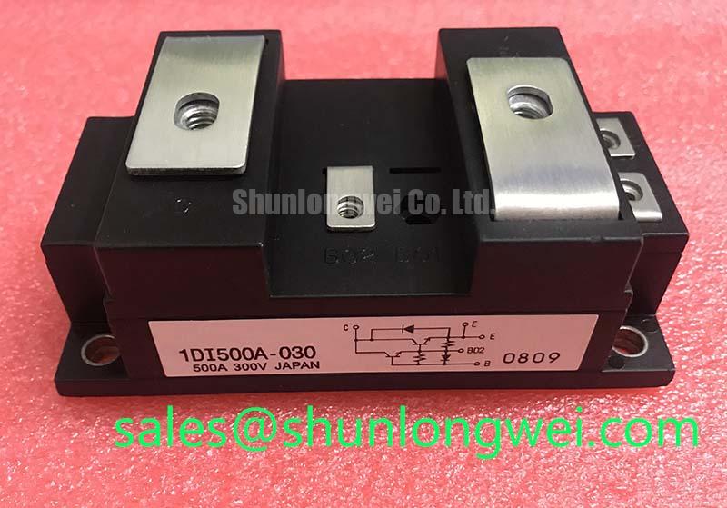
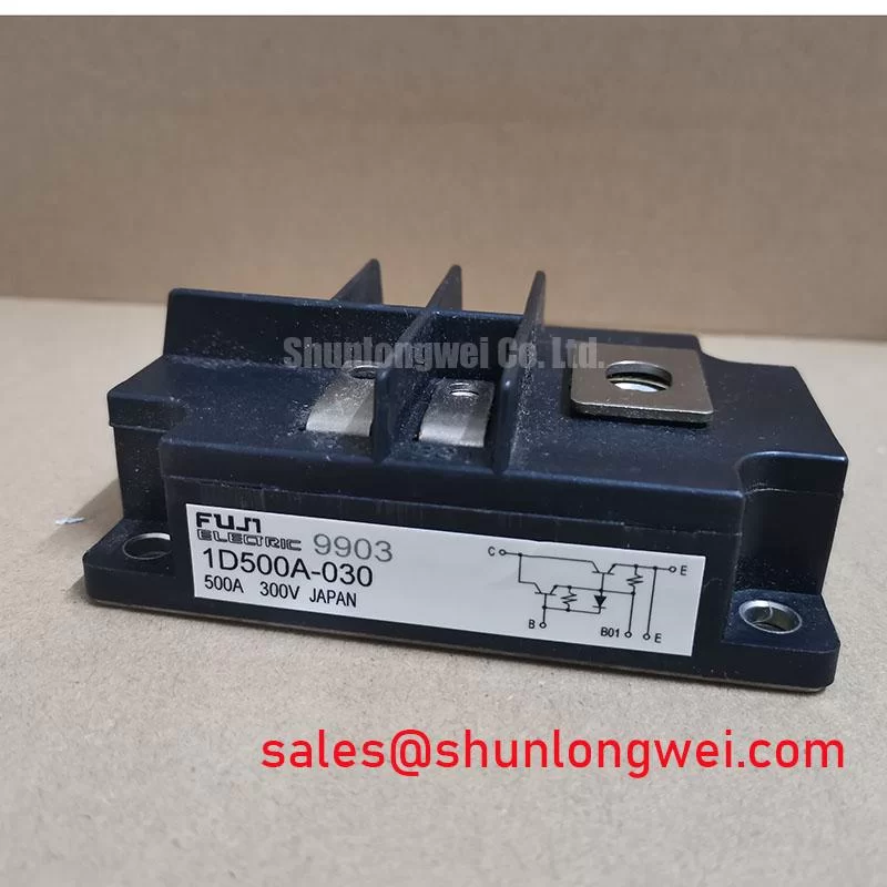
Isolate the DC link, confirm it is discharged, then compare the installed module’s terminal arrangement and mounting footprint with the replacement documentation before loosening the busbars. The 1D500A-030 is identified as a Fuji Electric IGBT module in a Fuji Power Module package, with a rated voltage of 2500 V and rated current of 500 A (Official Specification). Those ratings identify the part; they do not establish a permissible DC-link voltage, switching transient, or capacitor-bank layout on their own.
At the DC-link cabinet, inspect capacitor connections for loose joints, heat discoloration, and unequal conductor paths before attributing a shutdown to the module. As a Design Consideration, minimizing busbar loop inductance helps limit voltage overshoot during turn-off. The system engineer should measure the switching waveform at the installed operating conditions and check its peak against the module’s voltage boundary. Snubber selection and electrical clearances must follow the equipment design and applicable installation requirements rather than a presumed value for this part.
A commercial string inverter or micro-grid storage converter is a possible compatibility evaluation context, not a confirmed application for every 1D500A-030. For a repair, match the original circuit diagram, terminal functions, mechanical interfaces, cooling arrangement, and driver requirements. The listed 3MBI50SX-120-02 can be examined as a separate procurement comparison, but its suitability as a replacement cannot be inferred from its model number.
Field Diagnostics & Commissioning: Baseplate Thermal Grease Layer Control in 1D500A-030 Topologies
With the assembly de-energized, photograph the original busbar and driver connections, then check the removed module and heatsink for uneven contact marks, debris, and damaged mounting surfaces. A cold multimeter check between accessible power terminals may reveal a gross short, but it cannot certify the module for operation. Compare readings with the circuit diagram and, where available, a known-good assembly; connected capacitors and parallel paths can change what the meter displays.
For reassembly, a Design Consideration is to spread compatible thermal interface material evenly and avoid visible gaps or excess buildup. Confirm heatsink flatness, mounting sequence, and fastener torque against the equipment and module installation instructions; no grease thickness or mounting torque is established by the supplied specifications. Field Alert: Never loosen module terminals or disconnect the driver until the DC link has been isolated and verified discharged.
After mounting, inspect terminal alignment before tightening the busbars, and check that the driver harness follows its documented routing. During controlled commissioning, compare temperature indications, gate signals, and switching waveforms with the equipment’s baseline. A rising temperature indication may reflect contact quality, cooling performance, current loading, or a sensing issue; it is not a stand-alone diagnosis of the module.
Assembly Integrity & Layout Architecture: Implementing Static and Dynamic Current Distribution for 1D500A-030
If the equipment uses parallel power paths, verify that each path matches the original schematic before assuming the modules will share current. Busbar resistance, thermal contact, and driver timing can affect distribution. Do not assume a particular temperature coefficient or current-sharing behavior for the 1D500A-030 without its detailed electrical characteristics and operating conditions.
As a Design Consideration, keep comparable power paths and gate-drive paths consistent so that one position is not exposed to a different switching environment. If measured currents diverge, inspect joints and conductor routing, then compare gate waveforms under a controlled test. An unequal reading alone does not distinguish a driver fault from a connection or measurement problem. Fuji Electric’s IGBT module information provides broader product-family context; the exact module documentation remains necessary for pinout and electrical-limit checks.
1D500A-030 Thermal-Electrical Optimization: Active Miller Clamp Implementation Practical Tuning
Before changing gate-drive hardware, trace the installed driver’s turn-off path and confirm its connection to the module terminals against the original schematic. In a switching leg, a changing collector voltage can couple into an off-state gate; a low-impedance clamp is one possible system-level means of limiting unintended gate movement. Whether an active Miller clamp is appropriate, and how it is configured, must be determined from the driver design, the module’s detailed gate limits, and measured waveforms. The supplied 2500 V and 500 A ratings do not specify a clamp setting or negative gate bias.
When investigating a trip, capture the gate-to-emitter waveform and power-terminal switching waveform with suitable isolated measurement equipment, then compare them with a healthy operating path. Check driver supply behavior, isolation-device performance, and gate-loop connections before adjusting damping. Protection coordination also needs the equipment’s fault-clearing design and the module’s documented short-circuit limits; neither can be established from the headline ratings. For background on how switching topology changes commutation and fault investigation, see Resonant Topologies in Home Appliances without treating its appliance circuits as a wiring guide for this module.