Content last revised on September 19, 2026
Transient Dynamics & Electrical Design: Optimizing Heatsink Contact Pressure on EVK71-060D
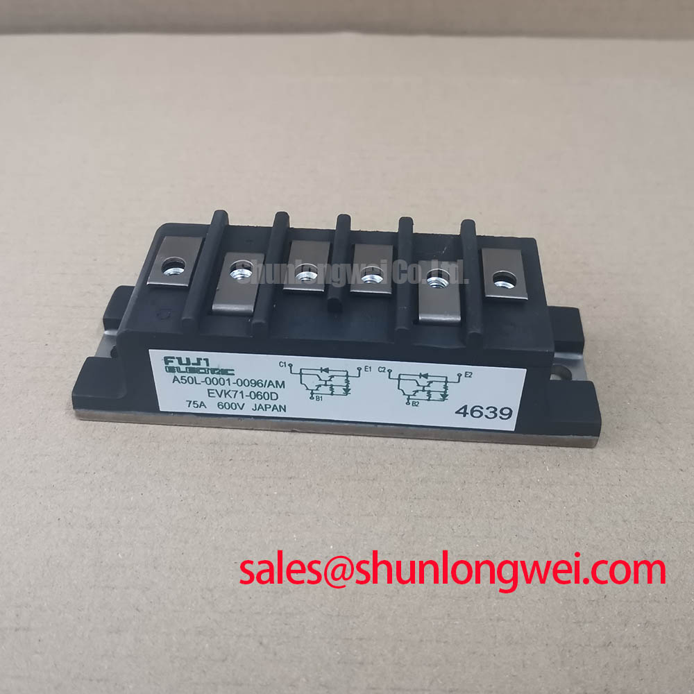
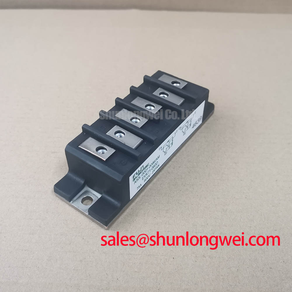
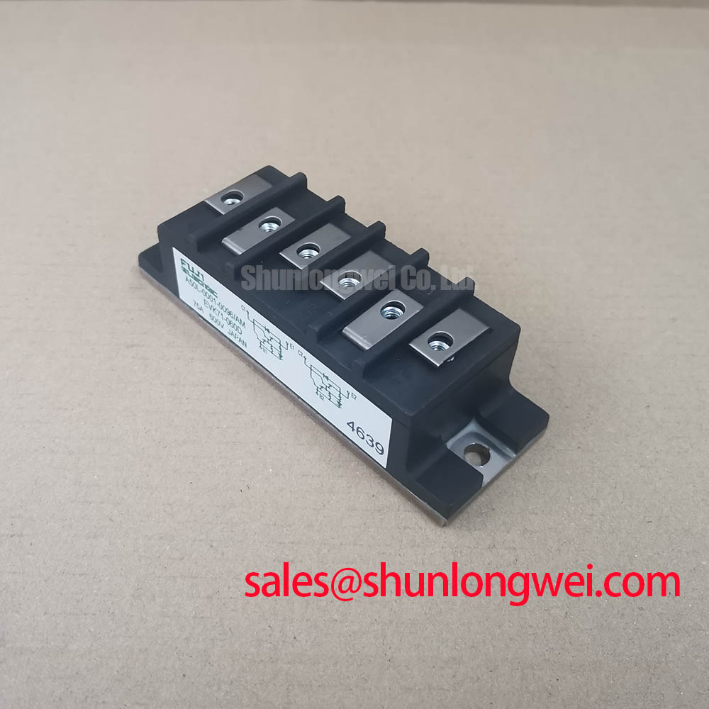
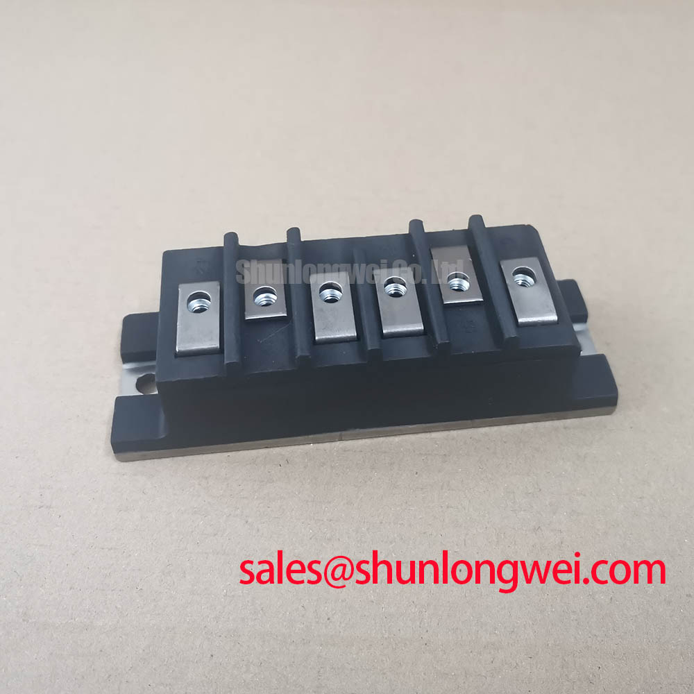
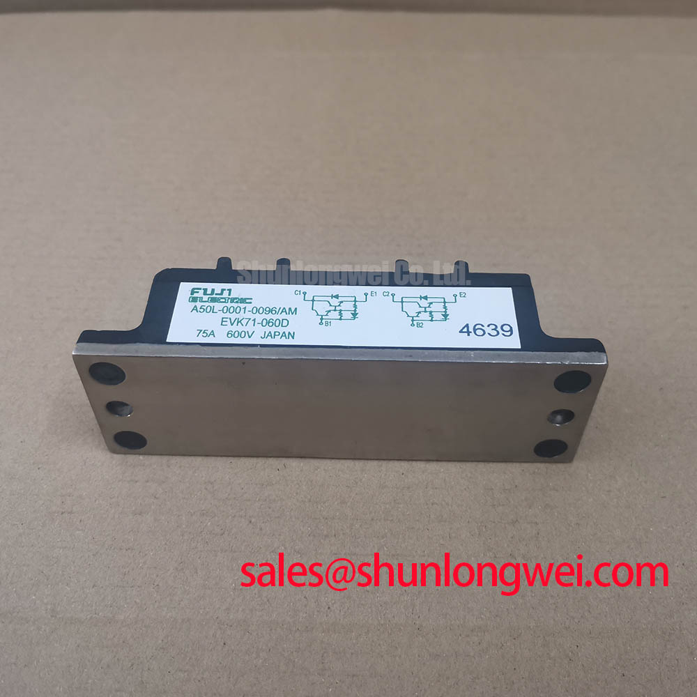
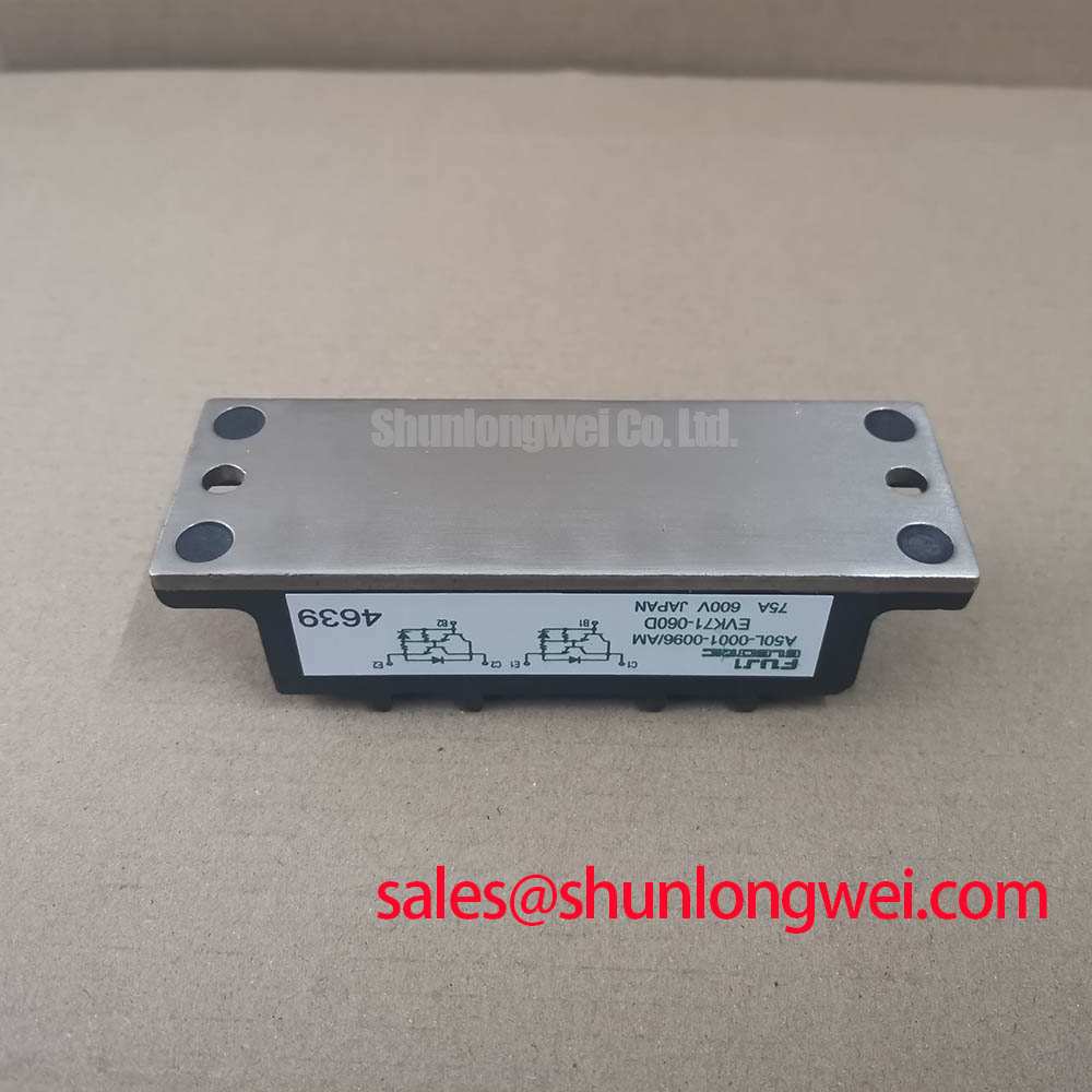
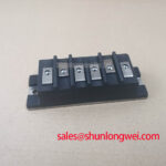
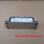
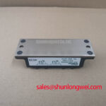
Start a replacement inspection by confirming the marking, checking the 600.0 V voltage class and 15.0 A rated current against the equipment documentation, then examining the Fuji power module base and terminals for mechanical damage before applying power. The listed product category is a Fuji Power Module; the supplied factory data does not define a complete pinout, switching-speed rating, thermal resistance, isolation rating, or gate-drive specification, so those values should be verified from the original module documentation before commissioning.
| Manufacturer | Fuji Electric |
| Model | EVK71-060D |
| Voltage rating | 600.0 V |
| Current rating | 15.0 A |
| Package | Fuji Power Module |
For heatsink installation, the practical objective is uniform thermal contact without bending the baseplate or stressing the ceramic substrate. A thin, continuous thermal interface layer is generally preferred, while excessive compound, trapped air, or contamination can increase thermal impedance. The proposed interface thickness must be selected from the actual surface finish, flatness, interface material data, and assembly process rather than treated as an EVK71-060D factory specification. If curvature compensation is required, the installer should resolve it through surface inspection and controlled mechanical assembly instead of forcing the module flat with excessive fastener load.
Use a sequential tightening pattern so the contact pressure develops evenly across the mounting points. The correct torque is a Design Consideration determined by the fastener size, module mounting instruction, heatsink material, washer arrangement, and thread condition. It is not supplied in the confirmed product data here. Safety interlock note: isolate and verify the DC link is discharged before touching the module, gate wiring, or heatsink assembly.
After installation, inspect the thermal interface perimeter, confirm that no compound has reached signal terminals, and check mechanical clearance around power and gate conductors. A thermal camera during a controlled load test can help identify uneven contact, but temperature interpretation should account for airflow, switching duty, sensor emissivity, and the actual case reference point. The Fuji Electric Power Semiconductors Portal provides manufacturer-level product-family context that should be used alongside the original technical documentation.
Transient Dynamics & Electrical Design: Output Sinusoidal Filter vs dv/dt Reactor on EVK71-060D
When evaluating the EVK71-060D in an industrial inverter welder or medium-frequency induction-heating power supply, separate the functions of a sinusoidal output filter and a dv/dt reactor. A sinusoidal filter is intended to reconstruct a smoother motor or load waveform, while a reactor primarily limits edge speed and interaction between the inverter, cable, and load. The suitable topology depends on switching frequency, cable length, load impedance, control response, and the voltage stress measured at the module terminals.
Long motor leads can behave as a transmission line. Reflections may increase terminal overshoot toward a multiple of the DC-link voltage in unfavorable installations, but the actual peak is system-dependent and must be measured with a properly rated differential probe. Do not use a nominal filter label as proof of semiconductor protection. Verify the worst-case turn-off and turn-on waveforms at the module terminals, including the effects of cable routing, grounding, load regeneration, and filter resonance.
The gate-drive loop deserves the same attention. Keep the drive and return paths compact, minimize shared inductance, and separate high-current commutation paths from sensitive control wiring. Gate resistance is a tuning variable rather than a universal EVK71-060D value. Designers should adjust sourcing and sinking behavior only after checking gate-voltage integrity, switching loss, overshoot, Miller-induced movement, and driver thermal stress. If ringing appears, compare the signal at the driver output and at the module gate terminals to distinguish wiring inductance from an unsuitable damping network.
In systems that also contain a thyristor front end, its IGT and VGT requirements belong to the thyristor data sheet, not to the EVK71-060D specification. A strong trigger pulse train may improve immunity to noise, but the pulse amplitude, width, repetition, and isolation must be established for that separate device. Likewise, bootstrap capacitor sizing and diode recovery behavior belong to the selected gate-driver architecture. The designer should verify recharge margin during the actual switching sequence, especially where common-mode ground bounce can disturb the high-side supply.
For a rectifier stage associated with the DC link, the 3MBI50SX-120-02 may be reviewed as a neutral reference for a related power-conversion position. It should not be treated as an automatic companion or replacement without checking topology, ratings, gate requirements, and mechanical compatibility.
EVK71-060D Operational Boundaries: Evaluating Thermal Time Constants and Peak Junction Limits
The confirmed data identifies a 600.0 V, 15.0 A module, but it does not provide the transient thermal impedance curve, junction-to-case resistance, maximum junction temperature, overload duration, or safe operating area. These missing values are decisive when the load contains pulsed welding current or intermittent induction-heating bursts. Engineers should obtain the applicable Fuji documentation before calculating a junction-temperature margin.
A useful bench method is to record case temperature, heatsink temperature, ambient conditions, DC-link voltage, current waveform, and switching frequency during the complete duty cycle. The thermal model can then use the manufacturer’s multi-RC data, if supplied, to estimate junction response across short pulses and longer repetition intervals. Without that curve, a calculated peak junction temperature would be an assumption rather than an official or validated result.
Thermal troubleshooting should begin with waveform correlation. If electrical loss rises, inspect switching overlap, gate ringing, diode reverse-recovery behavior, load commutation, and DC-link ripple before attributing the temperature rise to the heatsink alone. A reverse-recovery softness factor S, where available from the diode manufacturer, can help compare recovery behavior and potential EMI excitation; it cannot independently establish the thermal limit of this Fuji module.
Check the fast semiconductor protection path as well. A fuse selected for a high-power converter must be coordinated with the complete short-circuit response, including its I²t characteristic, wiring inductance, driver protection, and the module’s short-circuit withstand information if published. The absence of a confirmed EVK71-060D short-circuit duration means that dead-short testing should not be inferred from the 15.0 A current rating. Field measurements should be documented through the Field Engineer’s Handbook reference path and the equipment manufacturer’s procedures.
EVK71-060D Operational Boundaries: Evaluating Thermal Cycling Margins of Internal Braking Limits
For a braking chopper, first identify whether the equipment uses an internal braking transistor position or an external braking assembly. The EVK71-060D product information supplied here confirms voltage, current, and package category, but it does not confirm an internal braking topology, braking duty capability, resistor pulse rating, or energy absorption limit. The system engineer should therefore trace the actual DC-link schematic before assigning this module a braking role.
During deceleration, regenerated kinetic energy raises the DC-link voltage unless it is returned to the source, transferred to another load, or dissipated in a resistor. Resistor selection should be based on measured motor inertia, speed profile, stopping time, repetition rate, DC-link capacitance, and allowable bus-voltage envelope. The resistor’s pulse-energy and average-power data must be evaluated separately; a part that survives one braking event may not meet the thermal cycle imposed by repeated production stops.
Use an oscilloscope and isolated voltage probe to correlate the braking command, chopper gate signal, DC-link voltage, and resistor current. Unexpected bus rise may involve control delay, insufficient regeneration capacity, filter resonance, wiring inductance, or a protection threshold that does not match the system. The braking transistor gate loop should be routed to limit common-mode coupling, while the driver supply and any negative turn-off bias remain system-design decisions verified against the selected driver and module documentation.
For cross-reference work, the 6MBI15L-060 can be examined as a separate Fuji Electric module listing, but electrical, thermal, terminal, and mounting compatibility require direct verification before any substitution decision. The EVK71-060D remains identified by its supplied factory ratings of 600.0 V and 15.0 A; final braking validation should be based on measured bus transients, documented thermal behavior, and the original equipment protection scheme.