

Content last revised on November 6, 2026
Benchtop Waveform Tuning: Mitigating Gate-Loop-Induced Stress on FZ1500R33HE3
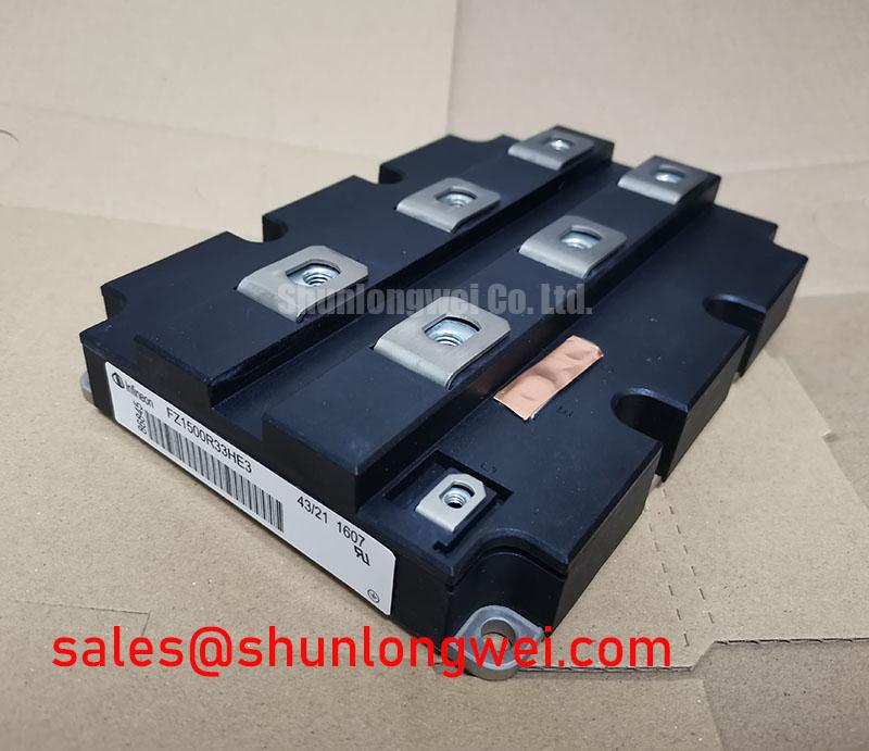
I trace the gate-driver return against the terminal drawing before connecting an oscilloscope to the FZ1500R33HE3, because a measurement referenced to the main emitter conductor can include voltage that the driver does not actually apply across the gate. With the equipment isolated and stored energy discharged, identify the collector, power emitter, gate connection, and any separately documented auxiliary emitter connection. Treat the terminal drawing—not connector position or a previous repair—as the authority for the driver return.
Design Consideration: distinguish the load-current path from the gate-control reference. Where the documented connection arrangement provides an auxiliary emitter return, route the driver return directly to that connection rather than through a shared power-emitter trace. Shared emitter inductance develops a voltage during current transitions, disturbing the effective gate voltage. This can contribute to oscillation or unintended turn-on, but a noisy trace alone does not establish the cause.
Measure gate-emitter voltage at the module connection using an appropriately rated differential measurement arrangement with a compact sensing loop. Compare it with the driver output while observing collector-emitter voltage and load current on synchronized channels. A disturbance present only at the module can point toward connection inductance or coupling; a disturbance already present at the driver warrants examination of its supply, reference, and isolation interface. Check probe placement before changing circuit components.
Engineering Recommendation: keep outgoing and returning gate conductors close together, separate them from the high-current commutation path, and assess clearance using the assembly’s insulation requirements. Gate resistance, turn-off bias, and any clamp function should be evaluated together against the approved driver and module limits. Negative gate bias is a system-level choice, not a value to infer from the 3300.0 V blocking rating. Compare changes under controlled switching conditions rather than selecting damping solely from an unloaded gate trace.
The power loop deserves a separate check. Closely coupled outgoing and return busbar paths can reduce stray inductance and the associated turn-off overshoot. Verify the resulting collector-emitter peak across the operating envelope, including protective switching events. The Infineon IGBT Modules & Discretes Official Portfolio provides manufacturer context for device families; switching limits and terminal details remain specific to the selected module documentation.
Field Diagnostics & Commissioning: PCB Symmetry Considerations for Dual IGBT in FZ1500R33HE3 Topologies
Separate the control returns of two externally connected switching positions before judging whether their PCB layouts are electrically symmetrical. The FZ1500R33HE3 is identified here as a single-switch IGBT; a dual-switch arrangement is therefore an assembly-level topology, not evidence of an internal half bridge. Similar-looking tracks do not guarantee similar switching behavior when their shared return paths, driver connections, and busbar geometry differ.
Design Consideration: compare each gate path from driver output to module and back to the driver reference. Where auxiliary emitter connections are documented, keep those returns outside the load-current routing. Examine coupling between adjacent switching positions, especially where one return passes close to the other position’s collector conductor. If oscillation changes when the neighboring switch operates, investigate mutual coupling and driver common-mode behavior before attributing it to the module.
Mechanical symmetry also matters during commissioning. Inspect the heatsink contact surface, remove residual interface material using an approved cleaning method, and check for burrs or contamination around mounting points. Apply the thermal interface material according to the qualified material and assembly process. Its appropriate thickness depends on surface flatness, material behavior, and mounting pressure; an arbitrary thin film or a heavy application can both compromise repeatability. Use a staged cross-pattern tightening sequence where specified by the mounting instructions, with calibrated tooling and the prescribed torque.
Maintenance Note: Trend terminal temperature rise and check cooling-air passages during scheduled maintenance before treating a warmer module as an internal semiconductor fault.
For replacement assessment, compare voltage class, circuit configuration, terminal geometry, cooling interface, and driver compatibility rather than matching current alone. The FZ1600R12KF4 can be included in a component comparison, but its inclusion does not establish interchangeability with this module. A substitution decision requires an electrical and mechanical review of the complete switching position, including protection coordination.
Likewise, place the FS75R12KS4 in a system review only where its own circuit configuration and ratings suit a separate converter stage. It should not be described as a front-end rectifier or complementary drop-in device merely because it is another IGBT module. For a potential utility-scale 1500 V central solar photovoltaic inverter application, designers should assess the FZ1500R33HE3 against the actual converter topology, DC-link excursions, cooling arrangement, and protection behavior rather than the equipment’s nominal voltage alone.
FZ1500R33HE3 Circuit Protection & Reliability: Evaluating Thermal Capacitance and Heatsink Response
Record the load-pulse duration and repetition pattern before using heatsink temperature to judge an overload event. A short electrical pulse can raise junction temperature before a case sensor or heatsink probe shows a comparable change. The 1500.0 A continuous collector-current specification therefore belongs in an operating-condition review, not as a stand-alone approval for a pulsed load or repeated braking event.
Engineering Calculation: for a rectangular loss pulse under the thermal model’s stated boundary conditions, the junction-temperature rise above the case reference is the pulse power multiplied by the junction-to-case transient thermal impedance at that pulse duration. A repetitive or variable loss history requires time-domain superposition or an appropriate thermal-network simulation. Use the manufacturer’s transient thermal data and model convention; fitted resistance-capacitance branches should reproduce that response rather than serve as invented physical layers.
Keep junction-to-case behavior separate from the interface and heatsink model. A multi-RC representation can describe transient response, but its connection to a cooling model depends on whether the supplied network is a Foster or Cauer equivalent. Combining networks without respecting that distinction can produce misleading junction estimates. Check the calculated temperature trajectory against measured case or baseplate behavior at the specified reference location and against the documented operating limits.
Design Consideration: when assessing a regenerative braking chopper, examine both semiconductor dissipation and the external resistor’s energy-absorption duty. A resistor that absorbs the bulk of regenerated energy does not remove the IGBT’s conduction and switching losses. Record the braking sequence, DC-link rise, switching pattern, and cooling response. Protection should account for resistor condition and energy duty as well as the switching device; adjusting the chopper threshold alone does not resolve a thermal-interface problem.
Maintenance intervals should follow contamination exposure and observed trends rather than a universal calendar. Compare airflow, coolant condition where applicable, mounting condition, and interface-material deterioration during planned outages. After a cold shutdown in humid surroundings, assess condensation before energization. A change in temperature rise at comparable load deserves investigation of cooling and electrical connections before any assumption about semiconductor aging.
The Deep Dive into Micro-Pattern Trench (MPT) Technology offers background on switching-loss mechanisms, but it does not establish that the FZ1500R33HE3 uses that technology or provide a service-life prediction for it. For product-family orientation, consult the Infineon IGBT Modules Overview; use module-specific loss and thermal information for the actual calculation.
FZ1500R33HE3 Thermal-Electrical Optimization: Failures-in-Time Assessment and Practical Tuning at High Altitude
Capture the sustained blocking voltage and switching peaks separately when evaluating a high-altitude installation. They represent different stresses: repetitive overshoot calls for commutation-loop and switching-control assessment, while a cosmic-ray reliability evaluation requires device-specific susceptibility information and the installation’s operating profile. Neither can be represented responsibly by subtracting a generic margin from the 3300.0 V collector-emitter rating.
Design Consideration: terrestrial neutron exposure is relevant to power-semiconductor reliability assessments, and installation altitude belongs among the environmental inputs. It is not appropriate to assign this module a universal altitude threshold, a fixed Single Event Burnout probability, or an altitude-based derating percentage without an applicable manufacturer model. Obtain the manufacturer’s cosmic-ray application guidance for the device technology and voltage class before assigning a numerical Failures-in-Time value.
A defensible assessment should identify the source of the susceptibility curve, its test conditions, the assumed neutron environment, and the time spent at each blocking-voltage condition. Include temperature dependence only where the source model supports it. Keep those inputs traceable in the equipment reliability file, and distinguish the modeled semiconductor contribution from cooling faults, connection degradation, and other assembly-level failure mechanisms. A calculated component contribution is not a measured fleet failure rate or a guarantee of operating life.
For practical tuning, first correct unnecessary electrical stress that measurements actually reveal. Reduce commutation-loop inductance where the mechanical layout permits, then reassess switching loss, overshoot, and gate disturbance together. Slower switching can reduce a voltage peak while increasing heat, so the adjustment needs both electrical waveforms and a thermal check. Any change to DC-link operating limits belongs to the system owner’s validated control and protection strategy, not to a distributor’s generic recommendation.
Retain the approved waveform captures, driver settings, thermal-interface process, and tightening records with the equipment maintenance file. At the next comparable operating check, compare temperature rise and switching behavior against that baseline. If altitude-related reliability is an acceptance requirement, close it with a manufacturer-supported assessment for the actual mission profile; use the commissioning measurements to establish the voltage and temperature inputs rather than substituting an unsupported FIT estimate.