




Content last revised on October 10, 2026
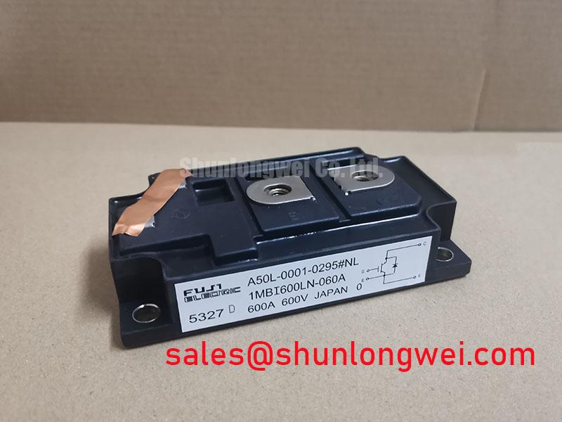
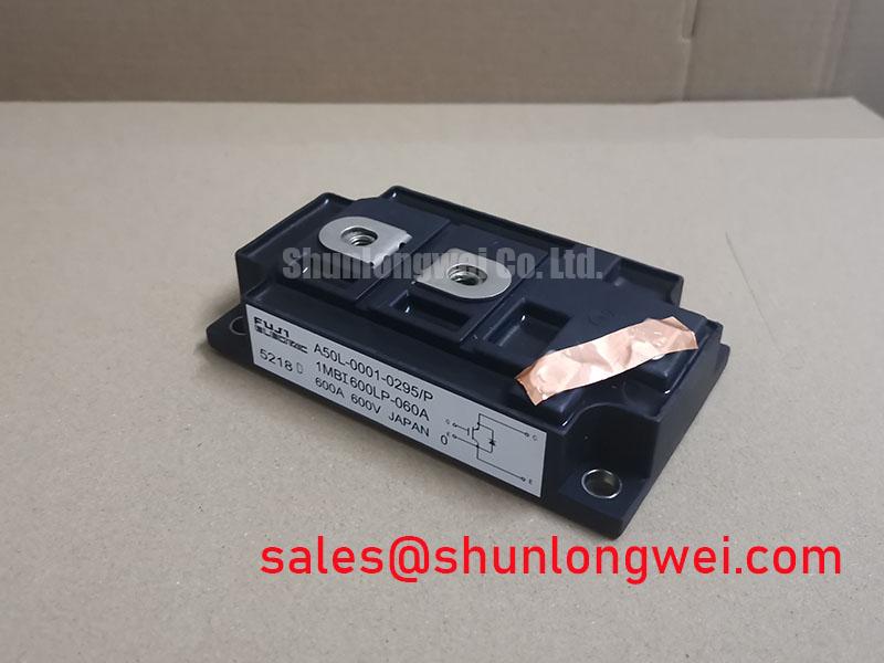
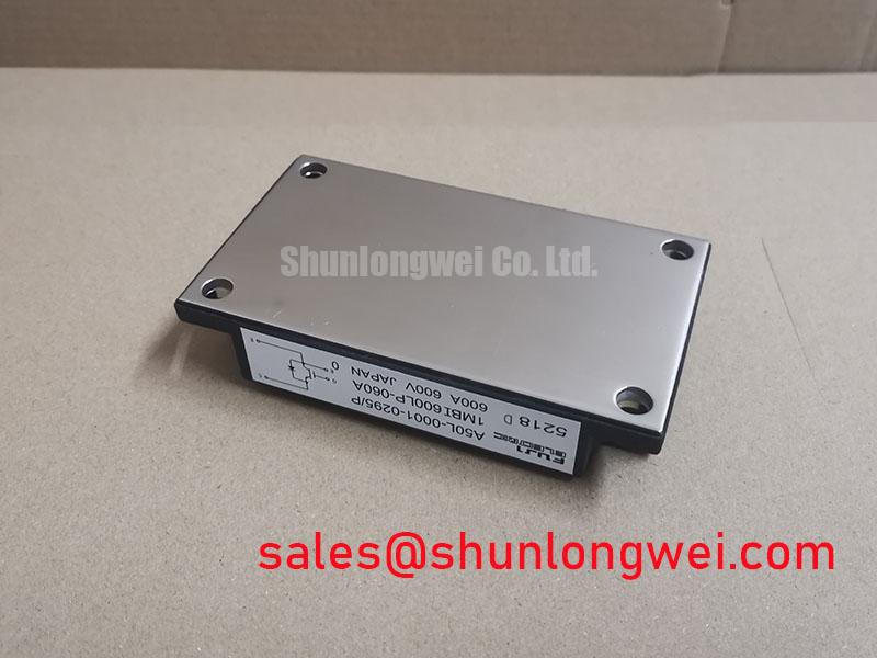
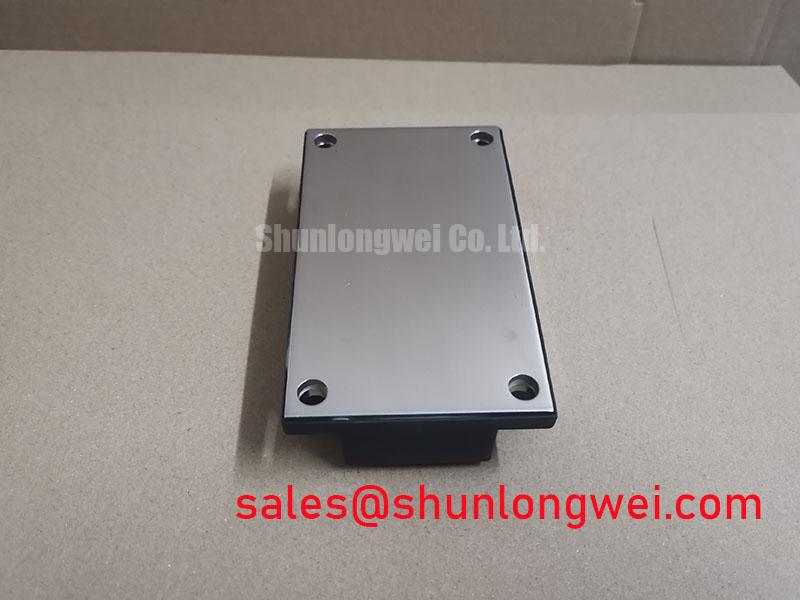
1MBI600LP-060 Fuji Electric 600V 600A IGBT Module
With the DC bus isolated, check the replacement module’s terminal markings, gate connections, and cold-state diode readings before it is connected to a legacy drive board. The 1MBI600LP-060 is a Fuji Electric IGBT Module with a specified voltage rating of 600 V and a rated collector current of 600 A under the applicable datasheet conditions.
These ratings identify the component class, but they do not by themselves establish suitability for every converter topology. A utility-scale 1500V central photovoltaic inverter requires a complete review of its switching arrangement, series or multilevel voltage sharing, gate-drive architecture, protection network, and insulation coordination. The 600V rating of this module must be evaluated against the actual voltage appearing across the individual switching position.
For procurement and incoming inspection, record the manufacturer, complete part number, package condition, terminal identification, and the measured cold-state results under controlled ESD conditions. The following guidance separates product ratings from practical engineering recommendations used during retrofit evaluation.
| Parameter | Value | Classification |
|---|---|---|
| Manufacturer | Fuji Electric | Product identification |
| Part number | 1MBI600LP-060 | Product identification |
| Voltage rating | 600 V | Device voltage rating, not a recommended DC-bus voltage |
| Rated collector current | 600 A | Subject to applicable datasheet conditions |
| Device type | IGBT module | Product identification |
1MBI600LP-060 Operational Boundaries: Evaluating Gate Drive Resistance
When a replacement module is installed on an older gate-drive board, begin by comparing the board’s gate resistor network with the switching behavior required by the replacement device. Separate turn-on and turn-off paths are useful because they allow the designer to control the competing effects of switching loss, voltage overshoot, gate ringing, and current transition speed. The correct resistance is system-dependent and should be established from the driver output capability, gate-charge behavior, isolation arrangement, and measured collector-emitter waveform.
A retrofit assessment should first identify whether the legacy board uses a single shared resistor, diode-separated resistors, an active gate clamp, or a negative off-state bias. Do not transfer the resistor value from another module simply because the voltage and current labels appear similar. Compare the gate-drive pulse at the module pins rather than at the driver output, since connector inductance, copper routing, and return-path impedance can alter the waveform seen by the gate.
During controlled switching tests, increase or decrease the external resistance gradually while watching turn-on current slope, turn-off voltage overshoot, gate plateau stability, and ringing after the transition. Excessive resistance can increase switching loss and thermal stress. Insufficient resistance can raise di/dt, aggravate parasitic inductance effects, and create false triggering through emitter return movement. The final setting should be validated under the intended DC-link condition and load current, not only during a low-energy bench pulse.
Keep the gate-drive loop compact and route its outgoing and return conductors together. The power commutation loop should be physically separated from the sensitive gate loop, while the driver reference should return to the designated module control terminal shown in the applicable terminal drawing. When a high-power solar inverter uses staged conversion or a multilevel arrangement, evaluate the switching position independently rather than treating the 1500V system label as the voltage across this 600V device.
For neutral comparison during an engineering review, the 2MBI300NK-060 may be examined as another Fuji module listing, but its electrical configuration and ratings must be compared directly with the original equipment requirements rather than assumed to be interchangeable.
Transient Dynamics & Electrical Design: Unpowered Multimeter Diode Screening on 1MBI600LP-060
Use the digital multimeter diode-check function only after the module has been removed from every energized circuit, and discharge the surrounding DC-link capacitors through the approved service procedure. Hold the gate shorted to the emitter during the main-terminal diode check to prevent a floating gate from turning the IGBT on and confusing the result. Probe the main terminals in both polarities to identify the expected one-way conduction path of the antiparallel diode associated with the tested switching section. The displayed forward reading is a screening result, not a complete semiconductor qualification measurement.
Repeat the check with consistent lead orientation, stable probe contact, and the same instrument used for the known-good reference. A large difference between comparable paths may justify isolation of the module for further examination, while an apparently normal diode reading does not verify gate integrity, dynamic switching performance, thermal behavior, or insulation coordination.
Gate leakage screening should be performed with the gate terminal isolated from the driver, clamp network, and surrounding board components, with the temporary gate-to-emitter short removed for this test. Check gate-to-emitter behavior in both polarities using a method appropriate for the device and laboratory safety limits. Avoid applying an uncontrolled external voltage to the gate during a basic incoming inspection. Any resistance or voltage reading influenced by parallel board components should be treated as a board-level result rather than a module result.
Dead-time and complementary interlock belong to the drive system, not to the module rating label. The upper and lower switches must not receive overlapping commands, and the dead-time buffer should be selected from measured driver delay, isolation delay, temperature variation, and turn-off behavior. Confirm the timing at the module control terminals with an oscilloscope before applying the working DC bus.
💡 Bench Tip: Use an ESD-controlled workstation and compare every cold-state reading with a documented known-good reference before installing the module in the power stage.
In a central photovoltaic inverter, the DC-link network, inverter bridge, and any input conversion, chopper, or clamp branches present in the design interact during transients. The 6MBI15LS-060 can be reviewed as a related topology reference, but it should not be treated as an automatic companion or replacement for this module.
Preventing Spurious Faults: Terminal Overheating and Periodic Inspection Guidelines for 1MBI600LP-060
Terminal heating should be investigated at the bolted interface, busbar geometry, current distribution, and cooling path rather than attributed to the semiconductor junction alone. A micro-ohmmeter can help compare the resistance of each assembled power connection, provided the test leads are arranged with a proper four-wire method and the measurement is made with the circuit fully isolated.
The proposed contact-resistance limit of less than 10 µΩ should be treated as a project acceptance criterion only when it is defined by the equipment manufacturer or assembly procedure; it is not an official rating supplied here for the 1MBI600LP-060. The useful diagnostic is consistency between equivalent joints, stable readings after mechanical assembly, and the absence of localized temperature rise during a controlled load test.
Inspect the mating surfaces for contamination, uneven pressure, damaged plating, busbar distortion, and fastener movement. A flat, properly supported busbar reduces mechanical loading on the module terminal. The heatsink interface also requires uniform contact and an even thermal path; excessive compound, tilted mounting, or uneven clamping can create a temperature gradient that appears later as a current-sharing problem.
Thermographic inspection should be performed after the assembly reaches a repeatable operating condition. Compare the power terminals, adjacent modules, busbar transitions, and heatsink regions using the same camera settings and viewing angle. A hot spot at one joint may indicate contact or current-spreading behavior, while a broader temperature rise may require review of switching loss, cooling airflow, duty cycle, or load balance.
For high-current service, periodic inspection intervals should be defined by the equipment maintenance plan, environmental exposure, vibration level, and thermal cycling history. The module’s 600 A rating is subject to the applicable datasheet conditions, while continuous application current remains dependent on the complete thermal and electrical design. Confirm the actual junction and case temperatures through the equipment’s approved measurement or estimation method.
1MBI600LP-060 Operational Boundaries: Evaluating Auxiliary Kelvin Emitter vs Main Power Emitter Connections
Do not assume that a control return terminal and a load-current emitter terminal are interchangeable. First match the physical terminal drawing for the exact module configuration, then trace the gate-driver return to the intended control reference. If an auxiliary Kelvin emitter is provided in the applicable configuration, it should carry the gate-loop return current separately from the high-current emitter path; if it is not provided, the driver layout must follow the documented terminal arrangement instead.
The purpose of a separate control return is to prevent voltage developed by load-current commutation from being interpreted as a gate-drive signal. Shared copper, long connector paths, and tightly coupled power conductors can introduce ground bounce into the gate loop. This may disturb the effective gate-emitter voltage during turn-on or turn-off and can produce irregular switching behavior that is not visible at the driver output pin.
Keep the control return routed with the gate conductor and connect the driver reference at the module interface selected by the device documentation. Avoid routing the control return through a busbar junction, current-sensing shunt, or high-current connector unless the system design specifically accounts for the resulting voltage. The isolation barrier, driver supply decoupling, clamp arrangement, and common-mode transient response should be reviewed together.
Where negative off-bias is part of the selected drive strategy, the turn-off path must be checked for adequate isolation, controlled transition behavior, and immunity to Miller-related gate movement. The technical reference Evolution of Negative Off-Bias Gate Drive Circuits provides relevant background for evaluating that circuit approach. Fuji Electric’s High-Speed Discrete IGBTs and Brake Chopper IGBT Modules pages can also support broader topology comparisons, while the final interface decision remains tied to the exact module and drive-board documentation.
Before energizing the inverter, verify command polarity, interlock behavior, control-return continuity, gate waveform symmetry, and the absence of abnormal ringing at the module terminals. For a 1500V central photovoltaic inverter, the system engineer must also confirm the voltage allocation across switching devices, surge suppression, insulation spacing, and the location of every clamp or MOV network before this 600V module is considered for a specific switching position.