
Content last revised on November 11, 2026
Assembly Integrity & Layout Architecture: Implementing Optocoupler vs Digital Coreless Transformer for 1MBI600LP-060A
With the DC link isolated and verified discharged, disconnect the power connections before checking collector-to-emitter resistance on the 1MBI600LP-060A; parallel circuitry can otherwise obscure the reading. Record the meter polarity, compare equivalent disconnected power stages, and inspect the gate connection before treating an unusual reading as evidence of module damage. A cold resistance check is a screening step, not a switching-performance test.
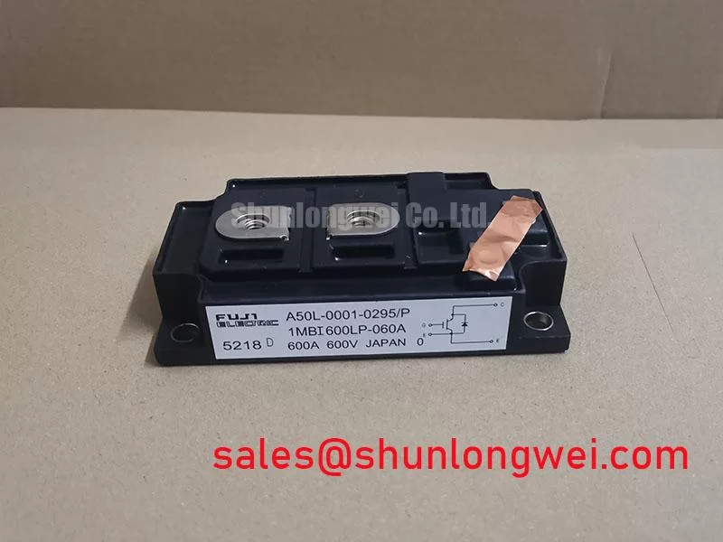
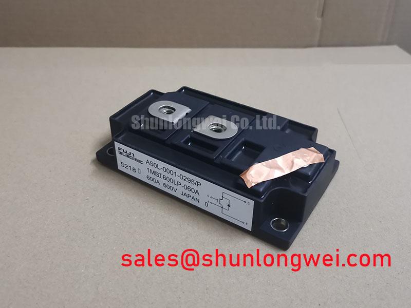
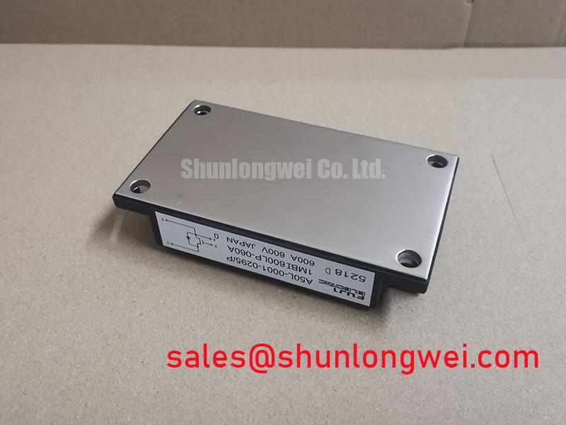
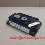
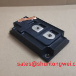
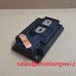
The Fuji Electric 1MBI600LP-060A is an IGBT Module with a Collector-Emitter Voltage (Vces) rating of 600.0 V and a rated Collector Current (Ic) of 600.0 A under the specified datasheet conditions. Those electrical ratings anchor the repair assessment; they are not sufficient by themselves to establish permissible operating conditions. Gate-driver behavior, terminal fit, cooling conditions, and protection coordination determine whether the surrounding equipment can return to service without repeating the original fault.
Trace the isolation barrier between the controller and gate-driver output before comparing optocoupler and digital coreless-transformer solutions. As a Design Consideration, the relevant comparison includes working-voltage capability, propagation behavior, common-mode transient immunity, isolated power-supply coupling, and the output state during supply interruption. The isolation technology alone does not establish suitability for this module or the equipment.
On the bench, examine the driver input and gate-to-emitter output together using appropriately rated isolated measurement equipment. A pulse appearing at the gate while the controller remains inactive warrants investigation of the driver supply, return-path impedance, coupling across the isolation barrier, and measurement setup. Check probe placement before assigning the event to the isolator: a long measurement loop can turn switching interference into an apparent gate transient.
Keep the gate-drive outgoing and return paths close together, separated from high-current commutation conductors where practical. The engineering objective is to limit coupled noise and gate-loop inductance under the actual switching conditions; clearance and creepage requirements remain determined by the equipment insulation design, environment, and applicable standards. Reinforced isolation is a property requiring documented assessment, not something established by an isolated voltage figure on a driver advertisement.
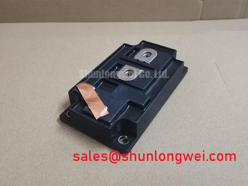
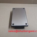
For the product record, the supplied specifications identify Manufacturer: Fuji Electric, Part Number: 1MBI600LP-060A, Package: Fuji Power Module, and Configuration / Topology: IGBT Power Stage. The electrical ratings are Collector-Emitter Voltage (Vces): 600.0 V and rated Collector Current (Ic): 600.0 A under the specified datasheet conditions. Package naming does not establish terminal dimensions, mounting interchangeability, or gate-drive requirements.
When reviewing device families, Fuji Electric’s High-Speed Discrete IGBTs page provides manufacturer context for a separate product category; it is not a specification sheet for this power module. Similarly, comparing the system role of 1MBI600U4B-120 requires its own electrical and driver assessment. Neither a related part number nor a shared manufacturer establishes a common gate-drive interface.
Transient Dynamics & Electrical Design: Fault-Clearing Dynamics: Type-I/II Desaturation on 1MBI600LP-060A
Check whether the protection circuit detects a short circuit already present at turn-on or one developing while the IGBT is conducting. These conditions, often described as Type I and Type II short circuits, place different demands on detection timing and current interruption. As a Design Consideration, review the complete fault path rather than the desaturation comparator alone: sensing, blanking, propagation, driver response, gate discharge, and fault latching all contribute.
Measure the desaturation signal alongside gate voltage and collector-emitter voltage during a controlled protection assessment. Blanking must reject normal switching behavior without concealing a genuine fault. Its duration belongs to the validated driver and device combination, not a universal repair setting. A generic short-circuit clearing time cannot be assigned to the 1MBI600LP-060A from its voltage and current ratings.
A staged or soft turn-off circuit can reduce the abrupt current change during fault interruption, but slowing the transition also prolongs electrical stress. Review the driver’s fault-discharge path, its supply stability, and the restart interlock together. Repeated automatic restart into an unresolved fault should not be used as a diagnostic method. Preserve the fault record and investigate the disconnected load and power circuit first.
For semiconductor fuse coordination, compare the fuse’s pre-arcing and total-clearing I²t characteristics with the protected circuit’s documented withstand conditions and prospective fault current. An IGBT current rating is not an I²t withstand rating. A semiconductor fuse and electronic desaturation protection address different portions of the fault sequence; neither establishes that a hard short circuit will be contained without a system-level coordination assessment.
During replacement evaluation, the following comparison keeps verified identity separate from unestablished interchangeability. The related 2MBI400NT-060 is a comparison candidate, not a drop-in replacement recommendation.
| Assessment item | 1MBI600LP-060A | 2MBI400NT-060 |
|---|---|---|
| Manufacturer | Fuji Electric | Consult datasheet |
| Collector-Emitter Voltage (Vces) | 600.0 V | Consult datasheet |
| Rated Collector Current (Ic) | 600.0 A under the specified datasheet conditions | Consult datasheet |
| Package | Fuji Power Module | Compare outline and terminal drawing |
| Configuration / Topology | IGBT Power Stage | Compare internal circuit diagram |
| Replacement approval checks | Gate characteristics, protection limits, cooling, and mounting interface | Independent electrical and mechanical assessment required |
For equipment compatibility, a utility-scale 1500V central solar photovoltaic inverter requires particular care: this 600.0 V module must not be treated as a device capable of directly blocking the full DC bus. Any proposed use depends on the actual stage topology and verified device stress, including transients. An equipment name on a purchase request is not sufficient evidence of compatibility.
1MBI600LP-060A Circuit Protection & Reliability: Calibrating Torque Reaction Absorption and Preventing Terminal Stress
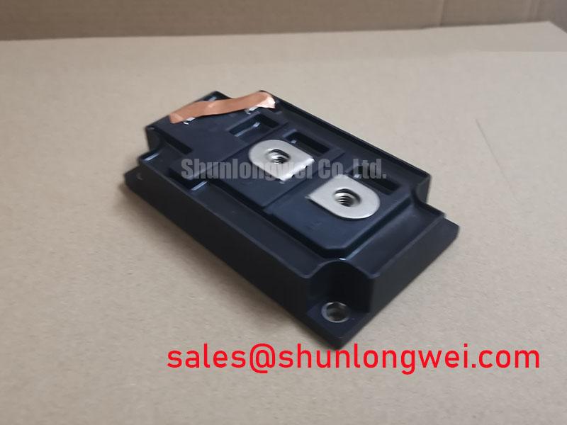
Offer the busbar to the module terminals without tightening it and check whether the contact faces sit naturally against each other. If screw force is needed to pull a displaced busbar into position, correct the alignment before assembly. As a Design Consideration, terminal fasteners should establish the intended contact pressure rather than compensate for an unsupported conductor or inaccurate mounting position.
Check the screw length against the actual terminal arrangement, including the conductor and specified washer stack. A screw that bottoms out can feel tight without producing the intended contact force. An unsuitable washer arrangement can also change engagement and loading. Use the applicable assembly drawing and terminal instructions to establish fastener selection and tightening conditions; the housing description alone supplies neither.
Field Alert: Do not use terminal screws to pull a misaligned busbar into place; support and align the conductor before tightening to the applicable assembly specification.
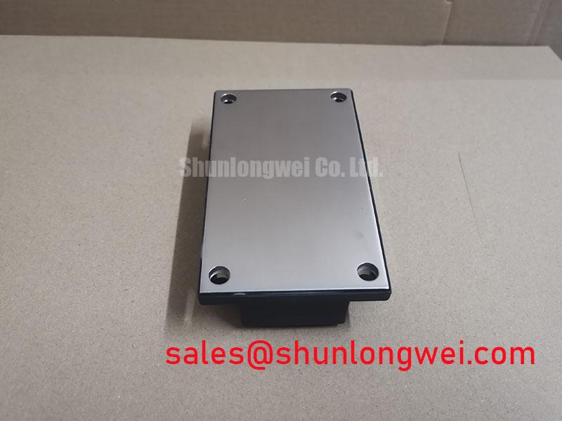
Inspect the heatsink contact surface for raised debris, damaged seating areas, and evidence of uneven previous contact. Apply the specified thermal interface material according to the equipment assembly procedure, keeping the contact layer consistent without using excess material to compensate for poor flatness. Tightening order and mounting load should follow the approved mechanical arrangement rather than an assumed torque based only on screw diameter.
After reassembly, inspect conductor support and cable strain throughout the service movement available inside the cabinet. Vibration and thermal movement should not turn a long busbar into a lever against the terminal. Where permitted by the equipment test procedure, compare connection voltage drop and temperature behavior under controlled load. An abnormal result can justify checking contact preparation, alignment, and current sharing; it does not identify a single cause by itself.
Record the installed part number, driver revision, terminal hardware, and thermal interface procedure in the repair handover. These details make subsequent measurements interpretable and prevent a later technician from comparing unlike assemblies. The Mastering High-Power SMPS guide offers broader circuit-construction context, while the replacement decision remains tied to this module’s interfaces and the equipment drawings.
Transient Dynamics & Electrical Design: Turn-Off di/dt Induced Peak-Voltage Clamping on 1MBI600LP-060A
Measure collector-emitter voltage at the module connection points during controlled switching tests, rather than assuming the DC-link measurement captures local turn-off stress. As an Engineering Calculation, the first-order relationship Vpeak = VDC + Lσ × |di/dt| explains why stray commutation inductance raises the turn-off voltage above the local DC-link level. It is an explanatory approximation, not a complete model of ringing or clamp behavior.
Reduce the enclosed commutation-loop area and keep the outgoing and return current paths closely coupled where the insulation arrangement permits. If a snubber is part of the design, its connection path matters as much as its nominal capacitance: a remote capacitor with an inductive connection may provide limited control of the fastest local transient. Select capacitance, damping, pulse capability, and placement from measured behavior and component limits, then assess losses across the operating envelope.
Examine the off-state gate waveform during the opposing switch transition. Collector-to-gate capacitance can couple displacement current into the gate circuit, creating unwanted gate-voltage movement. Reverse-transfer capacitance, commonly designated Cres or Crss, is not itself Miller plateau charge; both are operating-condition-dependent characteristics relevant to driver evaluation. For this module, do not substitute values from another Fuji device when assessing gate current or switching behavior.
As a Design Consideration, distinguish an active Miller clamp, which controls unwanted gate rise, from collector-voltage active clamping, which influences an overvoltage event. Their connections, activation conditions, and device stresses differ. Evaluate either function with the actual driver, local gate return, and power circuit. Fuji Electric’s Discrete IGBT & SiC MOSFETs resources provide additional technology context, but do not establish interchangeable drive or clamp settings.
If the existing equipment includes regenerative braking, distinguish energy absorption from transient suppression. A braking chopper and resistor manage returned load energy over the braking event; a local snubber addresses switching transients. Check the chopper command, resistor continuity, thermal protection, and DC-link response against the equipment procedure. Do not enlarge a snubber as a substitute for correcting a nonfunctional braking-energy path.
During the final controlled load assessment, capture gate voltage, collector-emitter voltage, current, and DC-link behavior under the relevant switching and regeneration conditions. Check probe ratings and connections before interpreting overshoot. If changing gate damping reduces a voltage spike, also evaluate switching loss and temperature behavior before accepting the adjustment; suppressing one waveform feature does not by itself establish an acceptable operating condition.