




Content last revised on September 30, 2026
Assembly Integrity & Layout Architecture: Implementing Negative Gate Bias vs Active Miller Clamping for 7MBP100RA060
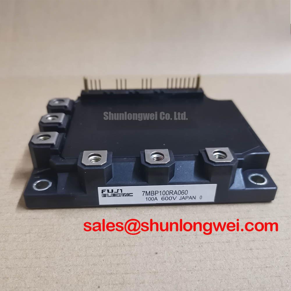
| Manufacturer | Fuji Electric |
| Part Number | 7MBP100RA060 |
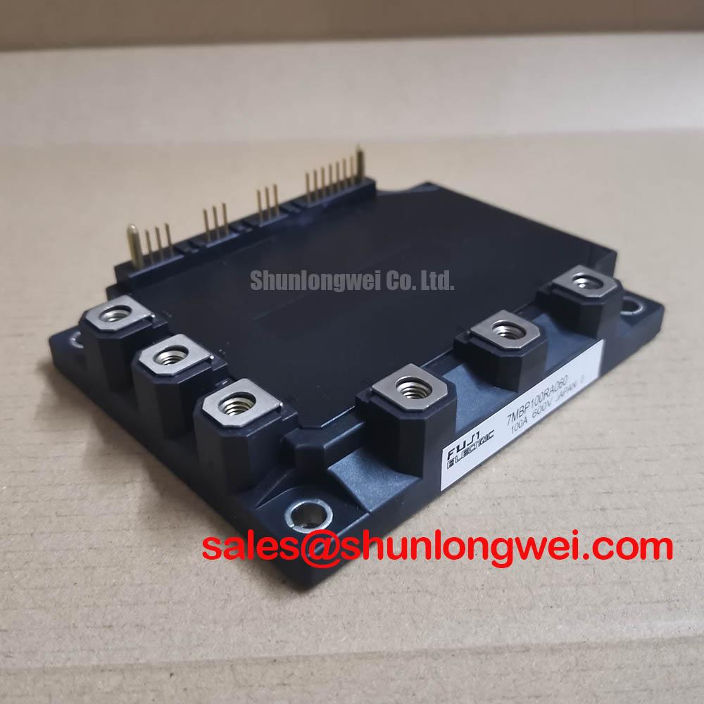
| Product Category | PIM intelligent power module with IGBT power switching and integrated protection |
| Collector Emitter Voltage | 600 V |
| Continuous Collector Current | 100 A |
| Isolation Voltage | 2500 V AC |
| Integrated Protection | Overcurrent, short circuit, undervoltage, and overtemperature protection |
Probe the gate to emitter voltage directly at the module terminals while observing the switching node with an oscilloscope; a clean gate waveform at the driver output does not prove that the same waveform reaches the 7MBP100RA060 under high current commutation.
The module is specified at 600 V collector emitter voltage and 100 A continuous collector current, so the gate-drive network must be treated as part of the power circuit rather than as a remote control accessory. Keep the turn-on and turn-off paths compact, avoid routing the gate trace beside high-current collector or emitter conductors, and provide a controlled return path to the corresponding emitter terminal. The correct physical arrangement depends on the module outline, driver topology, switching frequency, DC-link construction, and motor cable characteristics.
Negative gate bias is a system-level design option, not an assumed factory requirement for this part. If the selected gate driver supports a negative off-state voltage, the system engineer should verify the permitted gate-emitter limits, driver isolation, startup behavior, and fault-state response against the applicable Fuji Electric documentation. An active Miller clamp can provide another means of limiting unwanted gate rise during the opposite switch transition, but its effectiveness depends on clamp placement, driver current capability, common-emitter inductance, and the actual dv/dt measured at the power terminals.
During a field replacement, isolate the module and measure the gate-emitter path for abnormal low impedance before connecting the driver board. Compare each phase leg with a known-good leg using the same meter range and polarity. This is a screening operation, not a pass-fail substitute for a controlled gate-charge or switching test. If the gate waveform shows ringing, excessive overshoot, or a delayed return to the off-state, inspect the driver supply decoupling, gate resistor path, connector contacts, and emitter return before condemning the power module.
Clearance and creepage around the high-voltage switching terminals must be established from the working voltage, pollution environment, altitude, insulation system, and applicable equipment standard. The 2500 V AC isolation voltage rating is an official module specification; it does not by itself define the required PCB spacing or guarantee the insulation coordination of the assembled inverter. Engineers evaluating the part for electric forklifts or warehouse traction drives should assess enclosure contamination, cable routing, condensation control, and chassis bonding as part of the complete equipment design.
Use the neutral comparison link 7MBR100SB060-50 only when its voltage, current, protection, terminal arrangement, thermal interface, and control requirements have been checked against the existing inverter. A similar current class does not establish drop-in compatibility.
⚠️ Field Alert: Disconnect the DC link and verify the measured bus voltage has fallen to the equipment’s safe service condition before removing gate or power connectors.
7MBP100RA060 Thermal Electrical Optimization: Thermal Time Constants and Peak Junction Practical Tuning
Capture the case temperature, phase current, DC-link voltage, and switching waveform during the overload event instead of judging thermal stress from the heatsink surface alone.
The official continuous collector current rating is 100 A, but the usable current in an installed drive is determined by switching losses, conduction losses, ambient temperature, heatsink performance, airflow, mounting flatness, and the permitted junction temperature in the original technical documentation. A short overload can be thermally significant because the junction responds faster than the heatsink. For this reason, a transient thermal network with several RC time constants is more useful than a single steady-state resistance when assessing acceleration or lift transients in material-handling equipment.
In practical testing, log current and voltage at the same time as the module case temperature. Use the measured switching interval and duty pattern to identify whether the event is dominated by conduction loss, turn-on loss, turn-off loss, or recovery interaction with the freewheel path. The peak junction estimate is an engineering calculation only when the thermal impedance data, loss data, mounting condition, and initial temperature are known. Without those inputs, an apparently precise junction estimate can be misleading.
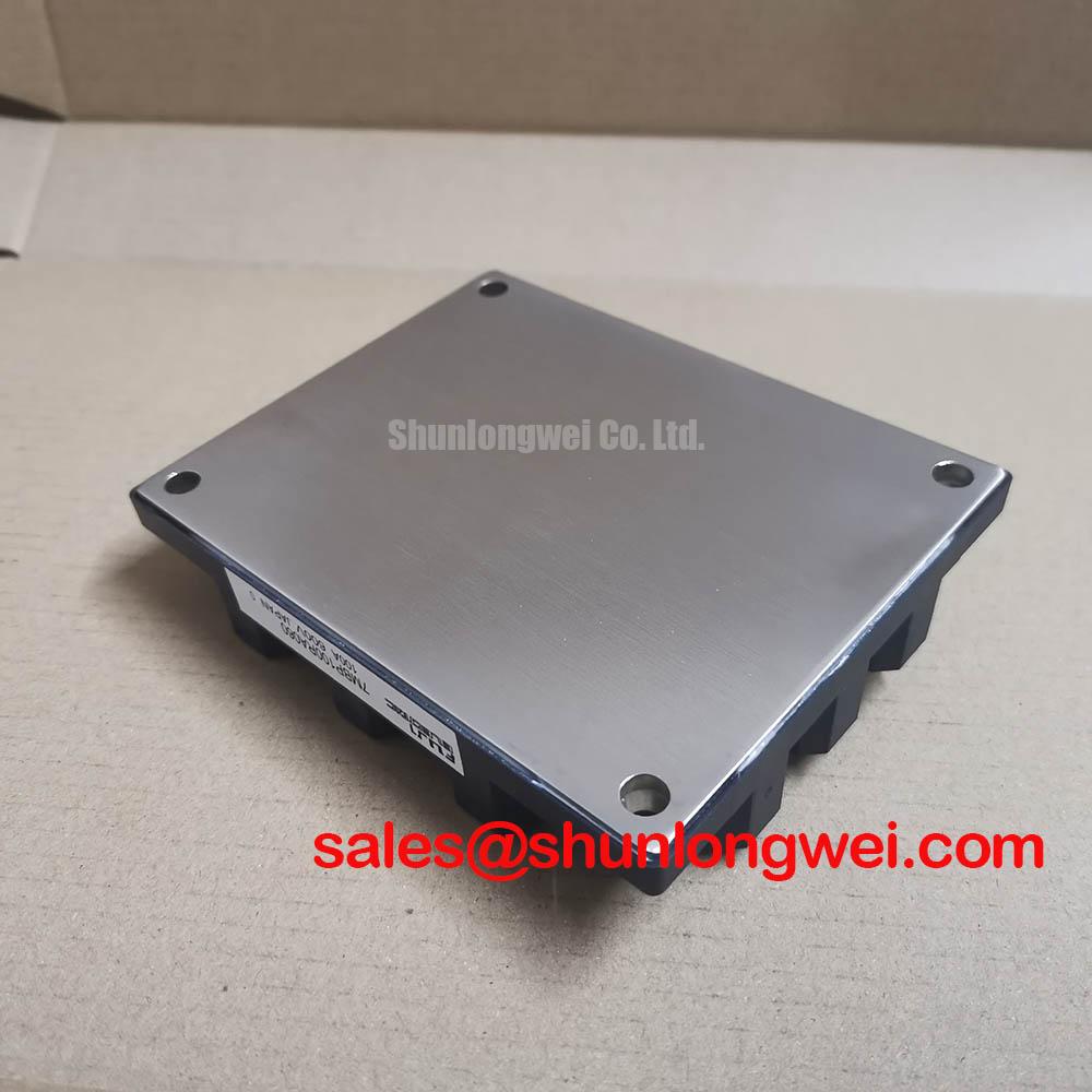
Inspect the thermal interface for voids, contamination, uneven compression, or a heatsink surface that does not contact the full mounting area. The interface material should be applied as a uniform, controlled film selected for the mechanical surface and approved thermal performance of the equipment. Mounting force should follow the original assembly instructions and fastener specification; do not substitute a generic torque value for the module manufacturer’s mechanical requirements.
When several modules or parallel current paths are used in the same converter, symmetrical busbar geometry and matched electrical path length help reduce unequal dynamic current sharing. The positive temperature coefficient associated with IGBT saturation voltage can support static sharing under suitable operating conditions, but it does not remove the need to check transient imbalance, stray inductance, gate-drive matching, and thermal coupling. Measure each phase path during the highest expected load rather than inferring balance from average input current.
Integrated overcurrent, short-circuit, undervoltage, and overtemperature protection can simplify the protection architecture, but the protection response still has to coordinate with the controller, gate driver, contactor logic, and fault-latch strategy. Confirm whether a protection event produces a latched shutdown, a controlled retry, or another behavior in the complete assembly. The module protection function should not be treated as a replacement for appropriate DC-link protection, current measurement, or safe discharge provisions.
For broader application context covering industrial power conversion and high-duty switching systems, engineers can consult the Industrial Applications reference. The thermal design remains equipment-specific and should be validated with the actual enclosure, heatsink, duty cycle, and ambient profile.
7MBP100RA060 Operational Boundaries: Evaluating PCB Gate Loop Layout Symmetry Limits
Compare the gate-emitter waveform at each phase position under the same test command, then inspect the auxiliary emitter return and main power emitter path for shared copper that can inject switching voltage into the control loop.
The gate driver senses voltage relative to its emitter reference. When the control return shares a high-current emitter trace, the voltage developed by parasitic inductance can appear as false gate feedback. That coupling may produce apparent gate ringing, uneven turn-off, or unwanted partial turn-on in the complementary device. The remedy is architectural: keep the low-current gate-drive return separate from the main commutation current path for as much of the layout as the module terminal arrangement permits, and join references only at the intended module interface.
Symmetry matters at the power terminals as well as at the gate resistors. Unequal copper length, different via counts, or a phase conductor routed close to a noisy switching node can create different turn-on and turn-off behavior between otherwise identical legs. During troubleshooting, exchange the driver channel or gate resistor position only in a controlled test and record whether the waveform follows the circuit position or remains with the power leg. This helps distinguish a channel issue from a power-layout issue without relying on a single assumed cause.
Use a properly rated differential probe for the switching node and a short, low-inductance probing connection for gate-emitter measurements. Long oscilloscope ground leads can create ringing that is not present in the equipment. Validate the measurement setup on a low-energy test condition before increasing the DC-link voltage. The observed waveform should be checked at the module terminals, not only at a remote driver connector.
The 600 V blocking rating defines an electrical boundary for the module, while the inverter layout determines how much switching overshoot reaches that boundary. Minimize the high-current commutation loop, position the DC-link decoupling according to the converter topology, and use snubber or clamp networks only after measuring the actual overshoot and its energy. MOV selection, if used, must account for continuous operating voltage, clamping behavior, pulse energy, repetition rate, and coordination with upstream protection; a MOV is not an automatic substitute for correct loop layout.
At the mechanical interface, verify that the module is seated evenly and that no busbar force is transferred into the power terminals. Misalignment can change terminal stress and disturb the intended conductor geometry. Check for loosened fasteners, darkened copper, cracked insulation supports, and connector retention problems after a fault event. These observations guide further testing but do not independently prove the failure mechanism.
Design teams requiring manufacturer-level semiconductor application information should consult Fuji Electric Global Power Semiconductor Technologies. Equipment-level safety and wiring practices should also be reviewed against the relevant standards framework, including resources from NEMA.
Benchtop Waveform Tuning: Mitigating Stress via Long Motor Lead Reflected Wave Voltage on 7MBP100RA060
Measure the phase voltage at the inverter output and again at the motor terminals with a suitably rated differential probe before adding a filter or changing the gate-drive timing.
Long motor leads behave as transmission-line structures at sufficiently fast switching edges. Their characteristic impedance, cable construction, motor input impedance, termination, and installation geometry can create reflected-wave behavior that raises the motor-terminal voltage above the local inverter waveform. A theoretical terminal peak approaching twice the incident step can occur in a severe impedance-mismatch condition, but the actual result depends on the complete cable and motor system. Treat this as a test condition to investigate, not as a fixed value for every installation.
For a forklift traction inverter or warehouse vehicle drive, first record the DC-link voltage, no-load switching waveform, loaded current, cable length, cable shielding, motor frame bonding, and operating temperature. Repeat the measurement during acceleration and regenerative braking because the active devices and freewheel paths can experience different voltage stress in each direction. Compare the highest measured peak with the 600 V collector-emitter rating and the system’s required transient margin using the original application limits.
Output chokes, dv/dt filters, sine filters, and damping networks should be selected from measured edge behavior, motor insulation requirements, allowable leakage current, filter losses, and control-loop interaction. Do not choose a filter solely from the motor horsepower or nominal current. A filter can reduce terminal stress while increasing switching loss or changing current-sensor behavior, so the modified system must be retested for module temperature, current ripple, protection response, and motor performance.
Check the DC-link busbars and local capacitors when the measured overshoot appears at the inverter terminals rather than only at the motor. Excessive commutation-loop inductance, poor capacitor connection, or an incorrectly coordinated snubber can increase stress on the module. Where a MOV or clamp network is used, verify its repeated pulse capability and clamping voltage across the complete operating temperature range. The protection system must be coordinated so that a fault does not leave the gate driver operating into an uncontrolled switching condition.
When a replacement module is installed, reproduce the original gate resistance, control interlock, phase sequence, motor-cable arrangement, and cooling interface before making performance comparisons. If the equipment uses a different driver board or cable route, compatibility must be evaluated as a system rather than inferred from the shared 100 A current rating. Final validation should include controlled switching tests, insulation checks, thermal observation, and fault-response verification at the intended DC-link conditions.