







Content last revised on September 5, 2026
1MBI600NP-060 Thermal Electrical Optimization and Reinforced Insulation Barrier Integrity
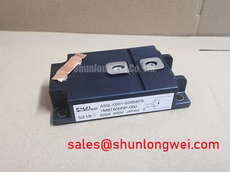
Begin a replacement assessment by isolating the inverter, confirming the nameplate limits, inspecting the module body and terminals, and checking the gate and power paths against the original wiring record. The Fuji Electric 1MBI600NP-060 is identified in the supplied factory data as a 600.0 V, 600.0 A IGBT Module in a module package. Those ratings establish the component identity and electrical boundary; they do not by themselves confirm suitability for every position in a utility scale 1500 V central photovoltaic inverter.
A 600 V module requires careful topology review in a 1500 V photovoltaic conversion system. Designers should verify the actual voltage appearing across the device during startup, normal switching, regeneration, fault interruption, and transient conditions. A module position connected directly to a 1500 V DC link cannot be accepted from the current and voltage label alone. The system engineer must confirm the converter topology, series device arrangement, clamping network, insulation coordination, and switching waveform before approving installation.
Reinforced galvanic isolation, common mode transient immunity, and gate driver isolation are system level verification topics unless the relevant Fuji Electric datasheet for the exact revision states specific values. Do not treat an assumed insulation rating above 5 kV or a presumed CMTI above 100 kV per microsecond as an official specification for this model without documentary confirmation. During commissioning, inspect isolation barriers, creepage and clearance around the mounted assembly, shield termination, and gate driver reference routing. A controlled hipot or insulation test should follow the equipment maker’s approved procedure and safety limits.
Spurious gate pulses can also result from driver reference movement, common source inductance, insufficient isolation performance, probe coupling, or an incorrectly referenced oscilloscope. Compare gate to emitter voltage at the module terminals rather than relying only on a distant driver test point. If a switching edge appears abnormal, measure the known good phase and the suspect phase under the same operating conditions, then review the gate resistor population, driver supply behavior, and turn off path. The measurement process should not expose the operator or test instrument to an unverified common mode voltage.
The freewheel path deserves equal attention. If the converter topology uses an antiparallel or external recovery diode, verify its reverse recovery softness, reverse current behavior, and specified operating conditions from the relevant diode documentation. A harder recovery event can increase commutation overshoot and radiated EMI, but the effect depends on stray inductance, gate timing, DC link impedance, temperature, and load current. The diode characteristics should therefore be evaluated with the complete commutation loop rather than inferred from the IGBT current rating.
Assembly Integrity and Layout Architecture for High Frequency Commutation
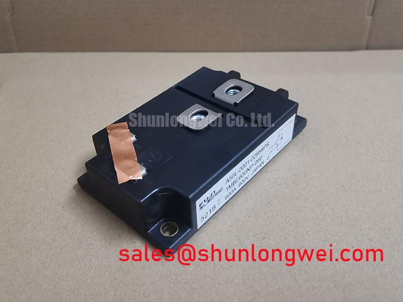
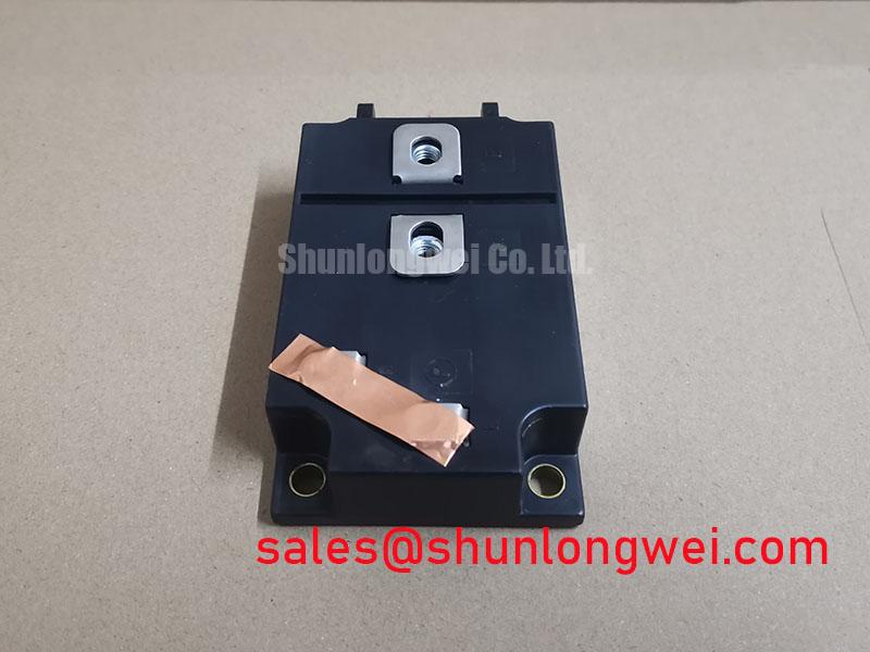
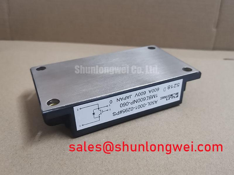
Before removing a failed unit, photograph the busbar orientation, gate wiring, auxiliary terminals, thermal interface, and fastener arrangement. This record helps prevent an apparently correct replacement from being installed with reversed polarity, displaced gate wiring, or uneven mechanical contact. The official physical data supplied for this listing specifies the package as Module; mounting dimensions, terminal assignments, internal circuit arrangement, and recommended torque should be checked against the exact manufacturer drawing for the purchased revision.
The principal layout objective is to minimize the high frequency commutation loop area. During turn off, stray inductance and current slew rate create an additional voltage across the loop, so the practical relationship between peak device voltage, DC link voltage, loop inductance, and switching rate must be checked using measured waveforms. The target inductance value must be determined by the system designer from the actual busbar construction, current profile, switching speed, and clamping margin. Do not apply an assumed value such as 25 nH as a guaranteed installation requirement for this module.
Use a compact, symmetrical laminated or planar busbar arrangement where the topology permits it, keep the forward and return current paths physically close, and position the DC link decoupling element according to the converter manufacturer’s layout rules. The oscilloscope probe connection should have the shortest practical loop and an appropriate common mode rating. A long ground lead can create ringing that is not present at the silicon terminals, leading to incorrect snubber or gate resistor changes.
Snubber selection is also determined by the measured ringing frequency, peak voltage, switching energy, capacitor parasitics, and thermal loss. Increasing capacitance may reduce a voltage peak while increasing turn on or turn off loss. Designers should tune the network from double pulse or controlled inverter tests, confirming semiconductor temperature and clamp stress at the intended operating point. The module’s 600.0 V rated voltage remains the official device boundary; a measured transient that approaches this limit calls for a system protection review rather than a simple assumption that the device will tolerate repeated exposure.
When several modules are connected in parallel, symmetrical copper resistance and inductance are essential. Static current sharing can be influenced by the positive temperature coefficient of on state voltage in many IGBT structures, but that behavior must not be treated as a substitute for balanced busbars, equal thermal paths, matched gate circuits, and controlled layout. Confirm current sharing with calibrated current probes and temperature measurements on each branch. A phase that runs warmer may reflect unequal mounting pressure, interface degradation, gate timing variation, or a different current path.
For broader design context, the IGBT Design and Integration resource can be used alongside the exact Fuji Electric documentation. Fuji Electric’s Brake Chopper IGBT Modules page also provides relevant manufacturer level application context, but it should not be read as a substitute for the specific 1MBI600NP-060 datasheet.
1MBI600NP-060 Circuit Protection and Reliability Through Thermal Feedback
Protection work should start with the actual fault sequence recorded by the inverter controller. Review gate driver fault logs, desaturation or overcurrent timing if available, DC link discharge behavior, phase current imbalance, and temperature feedback. A single alarm does not establish a single failed component. Check the module with the power removed, then inspect gate-emitter impedance, collector-emitter behavior, terminal condition, and the surrounding clamp and driver components using procedures approved for the equipment.
Thermal management is especially important at the 600 A class rating. The supplied factory information confirms the current rating as 600.0 A, but it does not provide a complete thermal operating point, case temperature, switching loss curve, or allowable overload profile. Actual current capability depends on heatsink performance, coolant or airflow conditions, switching frequency, pulse duration, duty cycle, junction temperature, and the manufacturer’s derating curves. Procurement teams should request the correct technical documentation before using the nameplate current as a continuous field operating target.
Inspect the heatsink for blocked passages, dust accumulation, corrosion, and evidence of uneven contact. Remove aged thermal interface material according to the equipment service procedure and check the mounting surface for flatness and contamination. Thermal cycling can loosen terminals or alter interface pressure, so compare terminal condition and fastener security with the original assembly record. Temperature should be monitored at comparable load points across phases; infrared readings require attention to emissivity and surface access, while embedded sensors require verification against the control system.
⚠️ Maintenance Note: Schedule periodic heatsink cleaning, verify airflow, and trend contact temperature under a repeatable load instead of relying only on an instantaneous alarm.
The gate circuit should be tested under low energy conditions before full power is restored. Verify driver supply stability, command polarity, dead time, turn off behavior, and the physical continuity of the gate and emitter return paths. If a high frequency gate waveform contains unexpected oscillation, compare it with the reference phase and inspect the probe arrangement before changing component values. Any suggested gate damping value is only a typical starting point for bench tuning; the final value is determined by the driver, wiring inductance, switching speed, and measured device stress.
For field replacement planning, the 1MBI200S-120 may be evaluated as a separate compatible device in applications where its own voltage, current, circuit configuration, package, and mechanical data satisfy the equipment requirements. It is not an automatic substitute for the 1MBI600NP-060. The responsible engineer should compare the original schematic, gate drive conditions, thermal interface, mounting pattern, protection thresholds, and manufacturer documentation before approving any alternative.
Preventing Spurious Faults Through Auxiliary Emitter Return Trace Separation
Keep the auxiliary emitter or driver reference return separate from the main high current emitter path wherever the module’s terminal arrangement and manufacturer drawing provide such connections. The purpose is to prevent load current induced voltage from appearing in the gate driver reference. If the auxiliary return shares a long section of the power emitter conductor, the driver can interpret the resulting voltage movement as a gate command disturbance, particularly during rapid commutation.
Route the gate and auxiliary emitter pair together with a controlled, compact geometry and keep it away from the collector busbar, snubber discharge path, and high current switching node. Avoid unnecessary loops, branch stubs, and shared connector pins with noisy power returns. The exact clearance and spacing should follow the equipment insulation design and the module drawing; generic layout numbers must not be presented as factory requirements for this model.
At the module terminals, inspect crimp quality, screw pressure, oxidation, connector insertion, and signs of heating. A loose auxiliary return can produce intermittent gate waveform distortion that appears only at load, temperature, or vibration. Compare the voltage measured directly between gate and the intended emitter reference with the voltage measured at the driver board. If the two waveforms differ materially, trace the return path and common mode coupling before replacing the module.
Bootstrap arrangements require the same discipline. A bootstrap capacitor and charging diode may be used in some high side gate driver architectures, but their presence and ratings are system dependent and should not be assumed for this module. Where such a circuit exists, verify capacitor high frequency charge and discharge margin, diode reverse recovery behavior, driver quiescent current, duty cycle, and low voltage lockout using the original driver documentation. An unstable bootstrap supply can imitate a gate fault even when the power module remains electrically serviceable.
After wiring corrections, perform a controlled low voltage switching test where the equipment procedure permits it, then increase operating conditions while monitoring gate-emitter voltage, collector-emitter voltage, phase current balance, heatsink temperature, and fault timing. Verify the peak voltage margin against the converter DC link during switching tests. Any EMC assessment must be made at the complete inverter level; the discrete module itself should not be described as independently certified to CISPR or EN 55011.