Content last revised on September 13, 2026
Field Diagnostics & Commissioning: Calculating Failures-in-Time Rates in 1MBI600UB-120 Topologies
| Parameter | Specification | Classification |
|---|---|---|
| Manufacturer | Fuji Electric | Product identification |
| Model | 1MBI600UB-120 | Product identification |
| Rated voltage | 1200.0 V | Official Specification |
| Rated current | 600.0 A | Official Specification |
| Package | Module | Official Specification |
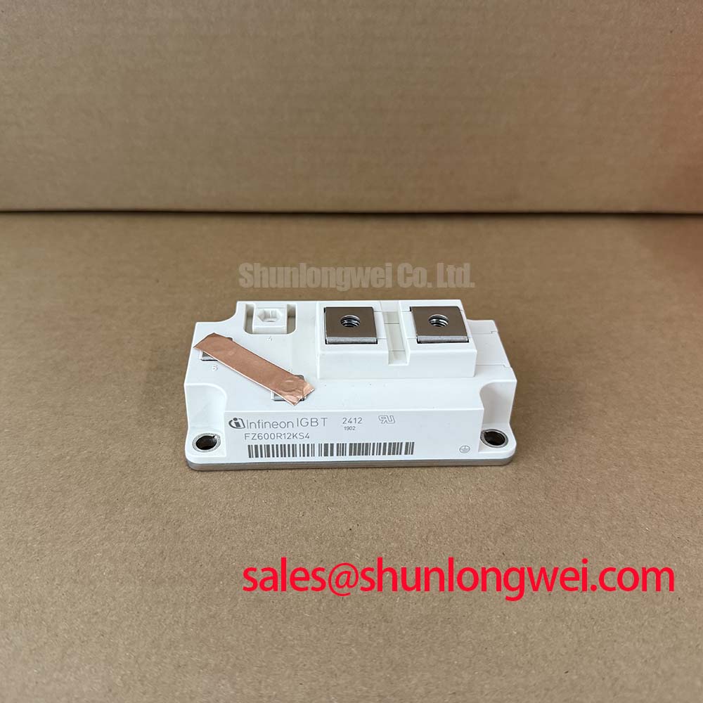
Begin a replacement assessment by isolating the converter, allowing the DC link to discharge, and checking the module marking against the service record before touching any power terminal. The Fuji Electric 1MBI600UB-120 is listed here as a high-current IGBT module with an official rated voltage of 1200.0 V, an official rated current of 600.0 A, and a module package. These values define the starting point for electrical compatibility review; they do not by themselves confirm suitability for a complete inverter, chopper, rectifier, or solar power-conversion assembly.
For field service, first document the failed switching position, gate-driver status, bus voltage, load condition, cooling condition, and the state of any parallel devices. A shorted collector-to-emitter path should be recorded as an observation rather than assigned to one cause. Compare the suspect position with a known-good phase using the same meter range and test arrangement, then inspect the gate-emitter path, driver supply, isolation barrier, snubber network, and mechanical contact to the heatsink.
The stated 1200.0 V rating requires particular care in a utility-scale 1500 V central photovoltaic inverter. A module carrying a 1200 V rating cannot be treated as a direct 1500 V DC-link switching device. It may only be considered within a separately verified lower-voltage conversion stage, auxiliary chopper, test platform, or another topology in which the applied collector-emitter voltage remains within the actual device and system limits. The system integrator should confirm blocking voltage, repetitive transient voltage, switching duty, current sharing, and insulation coordination from the complete Fuji Electric documentation before approving any use in that equipment.
Terrestrial neutron exposure and altitude can be relevant to power semiconductor reliability, but a defensible FIT or Single Event Burnout assessment requires device-specific test data, mission profile information, altitude exposure assumptions, applied voltage distribution, and an accepted reliability model. No device-specific FIT rate or SEB limit should be inferred from the nominal voltage and current values alone. At installations above 2000 m, treat reduced cooling performance, insulation coordination, creepage requirements, and atmospheric conditions as Design Considerations requiring system-level verification. Record actual operating waveforms and thermal conditions rather than applying an unsupported failure-rate multiplier.
During commissioning, use a controlled low-energy test sequence. Verify that the gate driver produces the intended command at the module terminals, check for abnormal common-mode movement, and confirm that the collector-emitter waveform remains within the approved device documentation during turn-on and turn-off. An oscilloscope with suitable differential and current probes is preferable to relying on a control-board indication. If a fault appears only under load, compare gate voltage, collector-emitter voltage, current rise, and temperature simultaneously so that electrical overshoot, insufficient drive, cooling restriction, and load-side fault conditions can be separated.
Fuji Electric application information for IGBT brake chopper modules can provide useful manufacturer context for chopper topologies, while the Fuji Electric IGBT product information should be consulted for current family documentation. These references do not replace the exact data required for this model and application.
Transient Dynamics & Electrical Design: Kelvin Emitter Connection on 1MBI600UB-120
Do not assume that a module has a separate Kelvin emitter terminal unless the exact terminal drawing confirms it. The supplied product information identifies the package as a module but does not provide a terminal map, internal circuit diagram, gate threshold specification, gate charge, or auxiliary emitter definition. The system integrator should verify the original Fuji Electric outline and terminal documentation before designing a driver return path around a presumed Kelvin connection.
Where a separately identified auxiliary emitter is available in the approved drawing, the Design Consideration is to return the gate-driver reference through that low-current sense path rather than through the main high-current emitter route. This reduces the possibility that common emitter inductance will appear as unwanted feedback in the gate loop. Keep the gate command and return conductors physically close, minimise the switching loop area, and prevent power commutation current from sharing the driver reference conductor. The final arrangement should be checked with oscilloscope measurements at the module pins, not only at the driver-board connector.
For a complementary half-bridge, dead time is a system-determined parameter. It must account for driver propagation variation, gate charge, turn-off behaviour, temperature, load current, and the measured tail current of the selected switching devices. A fixed dead-time value copied from another Fuji Electric module is not an official specification for this model. Interlock logic should prevent simultaneous commands, while the power and signal returns should be arranged so that common-mode ground bounce does not falsely trigger the opposing channel.
Negative off-bias may be evaluated where the switching environment, driver architecture, and transient behaviour justify it, but the required voltage must come from the approved gate-drive design and device documentation. It should not be inserted as a universal prescription. For practical maintenance and test reference, review Evolution of Negative Off-Bias Gate Drive Circuits, then verify gate-emitter limits, isolation requirements, and turn-off stability on the actual assembly.
When a returned module shows intermittent switching, inspect the driver connector, isolation power supply, gate resistor network, emitter reference, and control interlock together. A clean static gate reading does not prove stable dynamic operation. Compare the gate-emitter waveform during the same current transition on a known-good channel and check whether the disturbance is generated by the power loop or introduced through the control wiring.
Transient Dynamics & Electrical Design: DC-Link Capacitance Bank Layout and Low-ESR
The DC-link network should be reviewed as a complete commutation loop comprising the capacitor bank, busbar, module terminals, and return path. During turn-off, stray inductance and current slew can create voltage overshoot; the engineering relationship is commonly expressed as the DC-link voltage plus the inductive contribution produced by stray inductance and current change. The practical objective is to minimise the parasitic loop and confirm the measured peak voltage against the 1200.0 V device rating and the applicable transient limits in the approved datasheet.
A symmetrical laminated or planar busbar arrangement can reduce unequal current paths, but the correct geometry is determined by the module terminal pattern, capacitor construction, current waveform, insulation system, and mechanical enclosure. Do not impose a universal inductance target without a validated layout and measurement method. Place high-frequency decoupling where the switching loop requires it, keep the capacitor-to-module path short, and evaluate the effect of connection inductance rather than judging the bank by capacitance value alone.
Snubber selection also belongs to the switching test process. A capacitor and damping element should be selected after measuring the overshoot, ringing frequency, pulse energy, repetition rate, and temperature rise. A larger snubber is not automatically safer because it can increase turn-on current, switching loss, and capacitor stress. Designers should verify the network with a properly rated probe at the module terminals and compare the waveform across operating temperature and load conditions.
When diagnosing a converter that trips during fast load changes, inspect capacitor connection torque, busbar flatness, laminated insulation, current-sharing symmetry, and the condition of the damping network. Check the DC-link waveform both at the capacitor bank and at the IGBT terminals. A difference between those points may indicate layout or connection impedance that is hidden by a measurement taken only at the bank. Any application to a 1500 V central photovoltaic inverter must first establish whether this 1200 V module belongs in an isolated lower-voltage subsystem; direct placement across a 1500 V bus is outside the stated rating.
For neutral cross-reference work, engineers may review the 2MBI150UC-120 as a separate Fuji Electric product listing. It should be compared by voltage class, current conditions, circuit configuration, terminal arrangement, thermal data, and mechanical drawing rather than treated as an automatic replacement.
1MBI600UB-120 Circuit Protection & Reliability: Calibrating Dynamic Power Loss Dissipation and Multi-R
Thermal evaluation should begin with measured loss at the actual switching frequency, current waveform, conduction interval, gate-drive condition, and case temperature. The official data supplied for this page identifies voltage, current, and package, but it does not provide switching-energy curves, thermal resistance values, transient thermal impedance curves, junction-temperature limits, overload duration, or safe operating area. Those values must be taken from the applicable Fuji Electric documentation before calculating a permitted duty cycle.
A multi-RC thermal model can be used as an Engineering Calculation to represent the junction-to-case transient response, but its time constants and thermal resistances must come from the manufacturer’s thermal impedance data or from a validated test correlation. For a pulsed overload, integrate the time-varying device loss through the selected thermal network and compare the resulting junction-temperature estimate with the documented maximum. Do not convert the 600.0 A rated current into a universal overload capability; current rating depends on case temperature, cooling arrangement, pulse profile, electrical conditions, and the relevant test method.
In plant maintenance, inspect the heatsink fins, forced-air path, interface surface, mounting pressure, and thermal interface material condition during scheduled outages. Look for dust accumulation, oil contamination, discolouration near terminals, and evidence of uneven contact. ⚠️ Maintenance Note: Isolate and discharge the equipment before service, then monitor contact temperature under a controlled load while verifying the cooling airflow.
A rising case temperature with a stable electrical load should prompt checks of the thermal interface, fan performance, heatsink cleanliness, ambient temperature, and current imbalance. If the temperature rise is concentrated around one terminal, inspect busbar contact and fastener condition before attributing the result to semiconductor loss. Terminal rework should follow the equipment manufacturer’s mechanical specification because the correct tightening method and torque are not provided in the stated model parameters.
Protection coordination should include the gate-driver fault response, DC-link discharge path, semiconductor fuse selection, and short-circuit clearing behaviour. Fuse I²t coordination is system-specific and must be checked against the module’s documented short-circuit withstand capability, wiring impedance, prospective fault current, and protection clearing time. A fuse selected only from the nominal 600.0 A value may not provide suitable semiconductor protection. Any claimed short-circuit limit, service life, FIT rate, insulation capability, or safety certification requires a traceable manufacturer or standards-based source.