


Content last revised on October 28, 2026
Preventing Spurious Faults: Four-Quadrant Power Flow Guidelines for 2MBI100VA-060
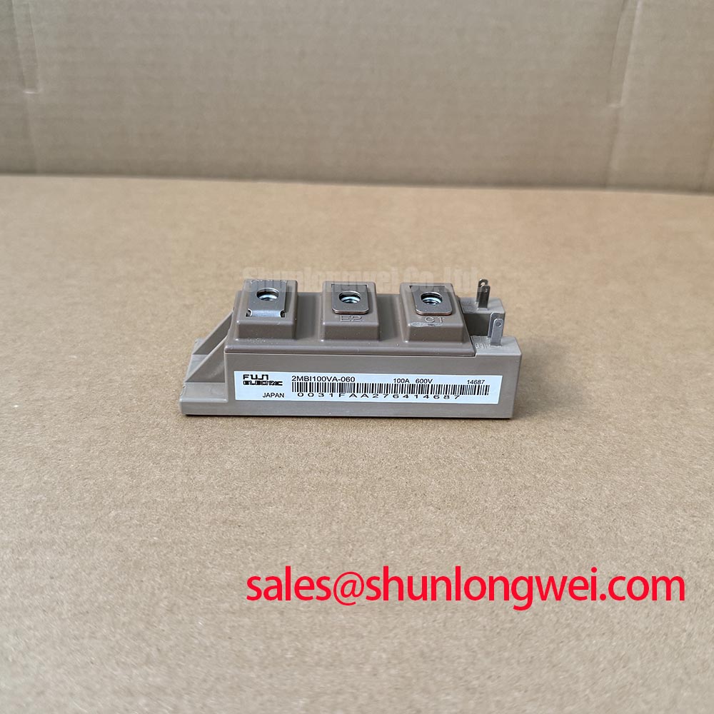
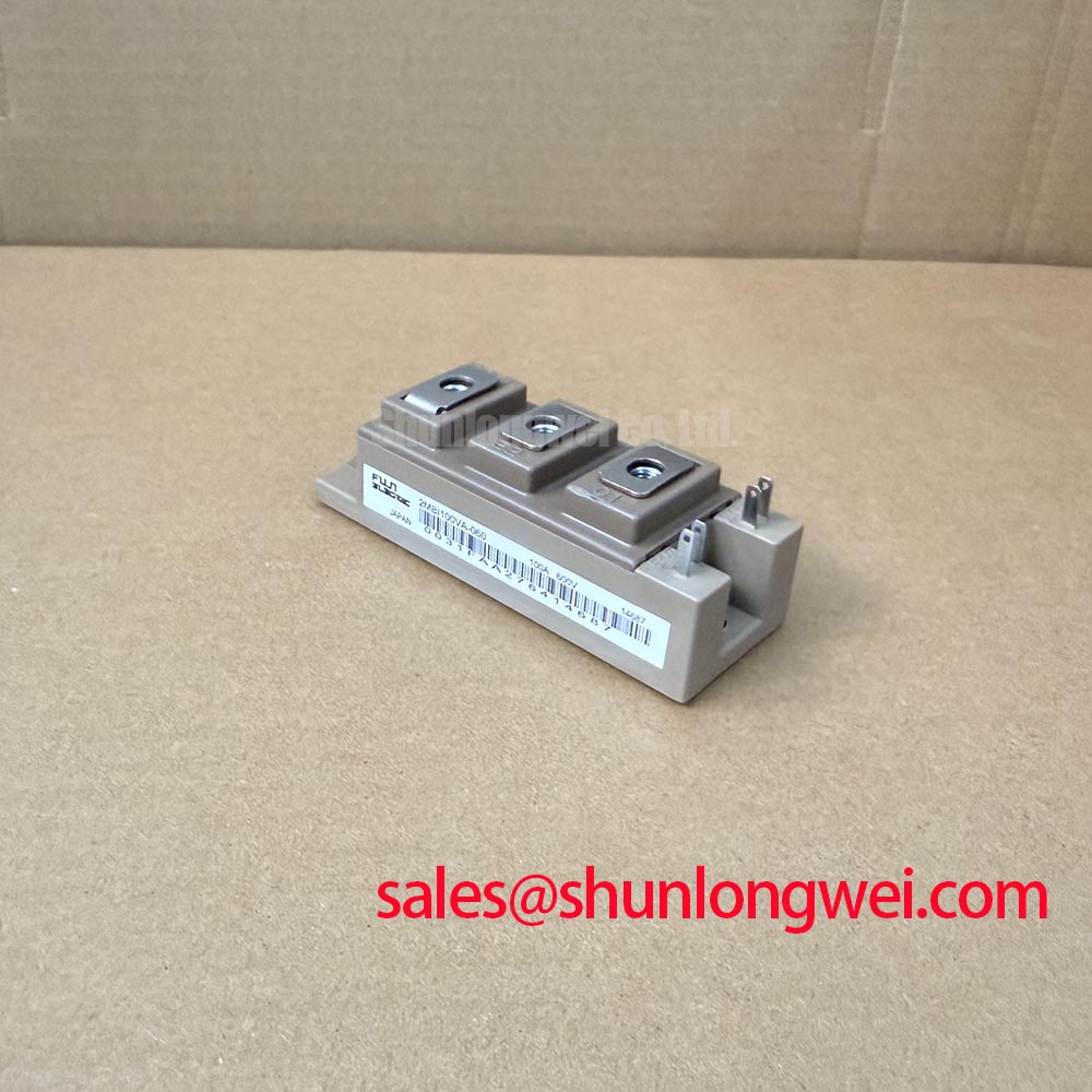
With the DC link discharged and the module isolated from its driver, match the terminal markings to the circuit diagram before placing a meter across the power terminals. For the 2MBI100VA-060 from Fuji Electric, the official specifications identify a collector-emitter blocking rating of 600 V at Tj = 25°C and continuous collector current of 100 A at Tc = 80°C. Record the case temperature alongside the electrical readings so subsequent comparisons use a consistent cold baseline.
The official collector-emitter saturation voltage is 1.70 V typical and 2.20 V maximum at Ic = 100 A, Vge = 15 V and Tj = 25°C. These are powered characterization conditions; a handheld meter cannot reproduce them. Incoming inspection should distinguish basic terminal screening from verification of the rated operating characteristics.
Trace the charging and discharging current paths separately before interpreting a direction-dependent protection trip. As a Design Consideration, four-quadrant operation belongs to the complete converter topology and its controls; an individual IGBT does not provide unrestricted bidirectional conduction and blocking. Identify when current passes through the controlled switching path and when it commutates through the associated freewheeling diode.
When evaluating compatibility with commercial string inverters or micro-grid energy storage converters, designers should check the battery-to-link conversion stage against the module’s electrical limits and actual switching conditions. During peak-shaving transitions, compare current direction, commanded switching states, case temperature and fault timing. A trip that appears during reversal warrants examination of commutation and sensing behavior before assigning the cause to the module.
The official junction-to-case thermal resistances are 0.26°C/W for the IGBT and 0.45°C/W for the freewheeling diode. Official total power dissipation is 480 W per IGBT at Tc = 25°C, with a maximum operating junction temperature of 150°C. The dissipation rating describes a specified thermal boundary, rather than an allowable continuous loss for an assembled converter.
As an Engineering Recommendation, evaluate pulse heating with the applicable transient thermal impedance characteristics and actual loss waveform. Steady thermal resistance alone cannot resolve short-duration junction-temperature peaks. Repeated load reversals also deserve attention at the mounting interface: Thermal Expansion Coefficient (CTE) Mismatch in Semiconductor Assemblies provides background on differential expansion, without establishing a service-life prediction for this module. Maintain the specified assembly contact conditions and assess temperature excursions under the intended duty cycle.
Assembly Integrity & Layout Architecture: Gate Driver Auxiliary Power Sequencing for 2MBI100VA-060
Check that driver readiness and undervoltage lockout inhibit switching while auxiliary supplies rise, fall or recover from an interruption. As a Design Consideration, the control sequence should establish a dependable off state before enabling the DC link and should preserve shutdown control while stored energy remains. Observe the gate-emitter waveform during supply transitions as well as during normal PWM operation.
If the equipment uses negative gate bias, verify its magnitude and transient excursions against the module’s gate limits and the driver specifications. The 15 V gate voltage in the saturation-voltage test is a characterization condition, not a complete gate-drive prescription. Negative bias, driver supply settings and protection thresholds remain system design choices requiring validation at the module terminals.
As an Engineering Recommendation, select driver sourcing and sinking capability together with gate charge, switching speed and external gate resistance. A stronger driver does not automatically produce cleaner switching. Examine turn-on and turn-off ringing, gate-voltage peaks and collector-emitter overshoot while adjusting damping within the approved design. Evaluate dead time against actual propagation delays and current commutation; excessive dead time can increase diode conduction, while insufficient separation can permit cross-conduction.
Keep the switching-current loop compact and assess any snubber or MOV network against measured transient energy and repetitive duty. Such networks complement layout and controlled switching behavior. The broader discussion in Unlocking Efficiency in Industrial Drives offers background on switching and loss tradeoffs; its technology-specific characteristics should not be transferred to this Fuji module.
Preventing Spurious Faults: Kelvin Emitter Connection Guidelines for 2MBI100VA-060
Trace the driver return to its emitter reference and identify any conductor shared with the main switching current. As a Design Consideration, voltage developed across shared emitter inductance can disturb the effective gate-emitter voltage. A waveform measured only at the driver output may therefore miss the disturbance experienced at the module.
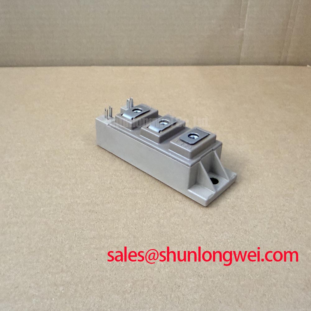
Establish the terminal functions from the module connection drawing before assigning an auxiliary emitter connection; the specifications listed here do not establish a dedicated Kelvin terminal. Where the documented terminal arrangement supports a separate driver return, route that return independently of the high-current path. Otherwise, assess the reference connection and shared conductor geometry without inventing an additional terminal function.
As an Engineering Recommendation, compare gate-emitter and collector-emitter waveforms using suitable differential measurement equipment and short probe connections. Correlate unexpected gate movement with current transitions, driver supply behavior and protection timing. This helps distinguish a gate-reference disturbance from a control command or a measurement artifact. Set conductor clearance and creepage through the equipment’s insulation requirements and applicable standards, rather than from the semiconductor blocking rating alone.
A replacement assessment should also compare terminal arrangement, mounting dimensions, driver compatibility and thermal interfaces. The 2MBI200VB-120-50 is a separate model for specification comparison, not an established interchangeable replacement. Likewise, Fuji Electric 7th-Gen X-Series IGBT Modules provides manufacturer product-family context without establishing that the 2MBI100VA-060 shares that generation’s construction or performance.
2MBI100VA-060 Operational Boundaries: Pre-Installation Junction Health Checks
Place the isolated module on an ESD-controlled bench, verify the meter’s lead polarity and identify each diode path from the connection diagram. As an Engineering Recommendation, hold the gate at emitter potential through an appropriate ESD-safe arrangement during static checks so incidental gate charging does not confuse collector-emitter readings.
💡 Bench Tip: Use ESD protection and compare readings with a known-good module at a similar temperature, keeping probe polarity and gate condition consistent.
Check each freewheeling path in both meter polarities and record the results rather than applying a universal pass threshold. The official diode forward voltage is 1.70 V typical and 2.20 V maximum at If = 100 A, Vge = 0 V and Tj = 25°C. A diode-check meter operates under different conditions, so its reading cannot verify that specification. Unexpected conduction in both directions warrants isolation from external paths and further investigation.
As a Design Consideration, a resistance check can reveal gross gate-terminal abnormalities but cannot establish compliance with a leakage-current limit. Formal gate-leakage testing requires the specified bias, polarity, temperature and instrument current compliance. Keep those results separate from the basic diode-screening record.
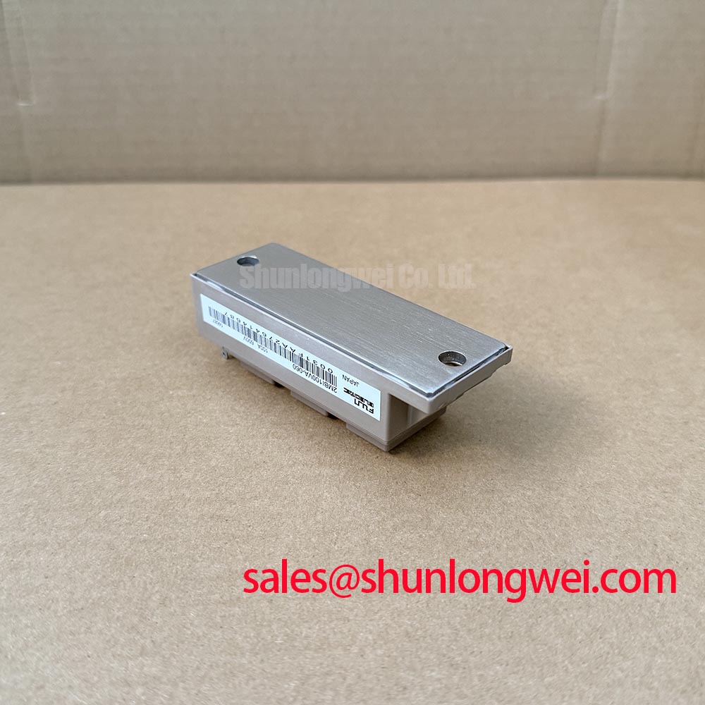
Check insulation between the designated electrical terminals and mounting interface only under the applicable manufacturer test procedure. The 600 V collector-emitter rating is not a terminal-to-baseplate dielectric withstand rating. Select test voltage, duration and acceptance criteria from the specified insulation test conditions; retain any abnormal reading for controlled investigation before DC energization.