




Content last revised on September 10, 2026
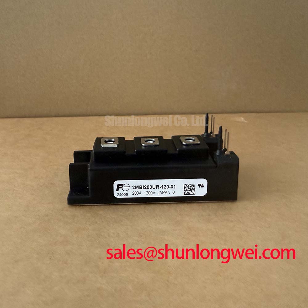
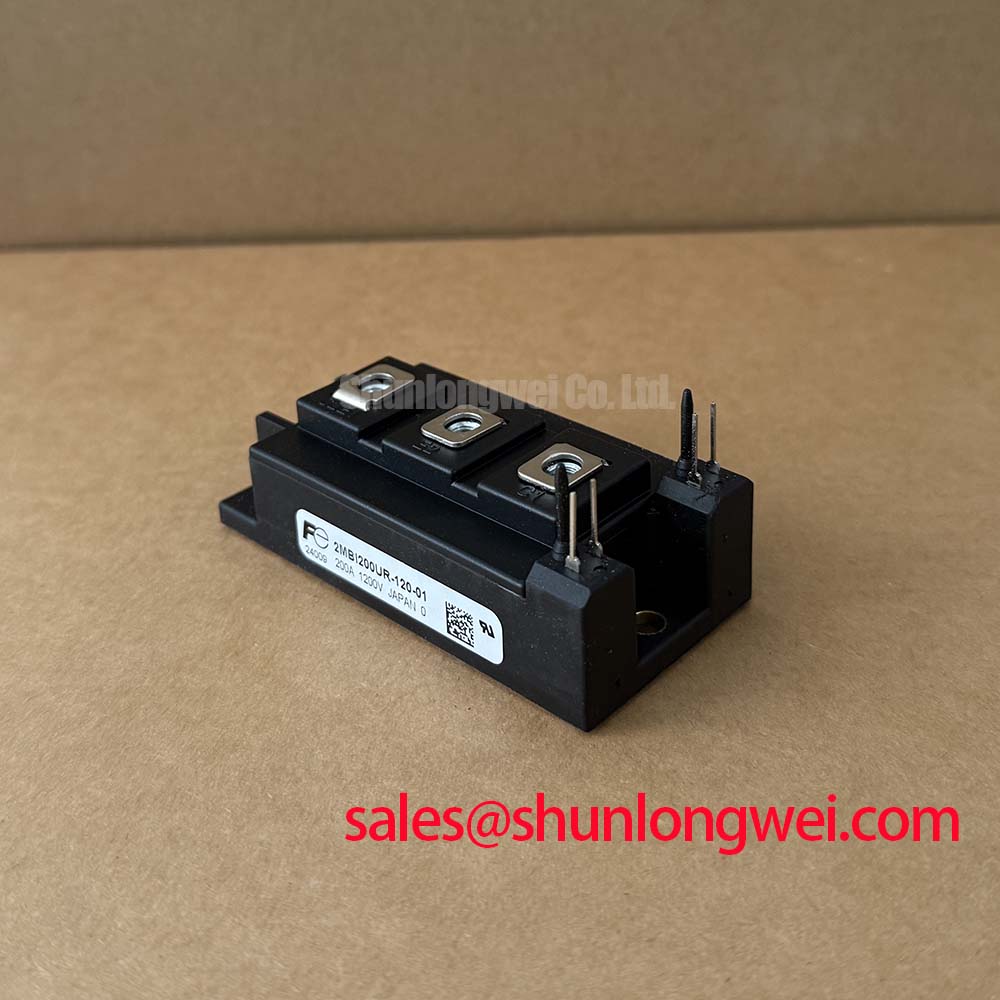
Fuji Electric 2MBI200UR-120-01 1200V 200A IGBT Module
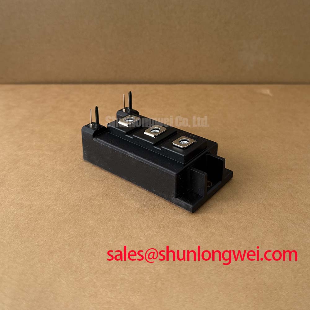
At the service bench, isolate the equipment, inspect the module body and terminals, and verify the nameplate rating before applying any test voltage; the 2MBI200UR-120-01 is a Fuji Electric IGBT module rated at 1200 V VCES and 200 A IC at TC = 80°C. This initial check helps prevent a rating mismatch when repairing a commercial string inverter, micro grid energy storage converter, industrial drive, or other high power switching assembly.
The published electrical characteristics identify a typical collector emitter saturation voltage of 2.10 V VCE(sat), a 10 µs short circuit withstand time, and an isolation voltage of 2500 V AC for 1 minute. These are official specification values supplied for this product page. They should be assessed together with the converter DC link, switching frequency, gate driver behavior, cooling system, fault response, and enclosure conditions rather than treated as a complete system rating.
| Parameter | Official specification | Engineering significance |
|---|---|---|
| Collector emitter voltage | 1200 V VCES | Voltage blocking capability relevant to industrial inverter and converter topologies |
| Collector current | 200 A at TC = 80°C | Current reference for thermal and electrical system evaluation |
| Collector emitter saturation voltage | Typical 2.10 V VCE(sat) | Important for conduction loss estimation and heat sink assessment |
| Short circuit withstand time | 10 µs | Protection timing reference before gate drive shutdown |
| Isolation voltage | 2500 V AC for 1 minute | Insulation test reference for the module isolation system |
The available specifications do not establish every mechanical detail, terminal arrangement, switching energy value, gate voltage limit, thermal resistance, or approved mounting procedure. The system integrator should verify those items against the original Fuji Electric documentation and the physical construction of the equipment being repaired. Fuji Electric’s semiconductor information can be reviewed through Fuji Electric Power Semiconductor and IPM Modules.
Transient Dynamics and Electrical Design: Junction to Case Thermal Network Simulation
For a replacement assessment, begin with the actual duty profile rather than the nominal current alone. The official 200 A collector current rating at TC = 80°C is a defined reference condition, while a commercial string inverter or micro grid energy storage converter can impose repeated load changes, charging transitions, regenerative events, and fault recovery pulses. The maintenance engineer should record case temperature, heat sink temperature, switching waveform, and phase current during controlled testing. Peak junction temperature must then be evaluated through the manufacturer’s thermal data and the complete junction to case, case to interface, and interface to heat sink path.
A multi section RC thermal model is an engineering calculation method for estimating transient junction temperature under pulsed loading. The model should use verified thermal impedance data for this exact module and the measured pulse profile. If those values are unavailable, a precise junction temperature claim would be unreliable. A practical engineering recommendation is to compare the calculated temperature trend with case temperature measurements and infrared inspection, while recognizing that surface readings can differ from the semiconductor junction.
The typical 2.10 V VCE(sat) value is useful for a first conduction loss estimate, but actual loss depends on collector current, junction temperature, gate conditions, and switching behavior. Designers should calculate conduction and switching losses separately, then confirm the result through calorimetric or temperature testing. A rise in contact temperature during an otherwise stable load may justify checking heat sink flatness, interface material condition, clamping uniformity, airflow, and terminal resistance.
High voltage layout should preserve the original equipment’s creepage and clearance arrangement. The module’s 2500 V AC isolation rating for 1 minute is an official isolation specification, not a substitute for the required system insulation design or pollution environment assessment. Keep power conductors, control wiring, and exposed conductive hardware arranged according to the applicable equipment standard and the original assembly geometry. The final spacing requirement is system determined and should be verified during the applicable dielectric and insulation tests.
Do not assume that a particular auxiliary or Kelvin emitter terminal exists, or assign its function from a similar Fuji Electric part. Confirm the terminal drawing before separating power emitter and gate return conductors. Where the original module provides a dedicated auxiliary emitter connection, the gate driver return should follow the documented topology and remain physically separate from the high current emitter path. An oscilloscope comparison between the gate to emitter signal and the power loop waveform can help identify common emitter inductance, ringing, or an unexpected turn off disturbance.
Thermal interface material should cover the intended baseplate contact area without contamination, voids, or excessive accumulation at the edges. The correct compound, application method, layer control, heat sink flatness, and mounting torque must come from the module documentation or equipment service specification. ⚠️ Maintenance Note: Check fan and heat sink cleanliness during scheduled service, then monitor contact temperature and recheck terminal tightness after thermal cycling.
Assembly Integrity and Layout Architecture: Desaturation Detection
The 10 µs short circuit withstand time is an official specification and should be treated as a protection coordination reference, not as permission to delay fault shutdown. The gate driver, desaturation detector, blanking behavior, soft turn off circuit, isolation barrier, and fault latch must be evaluated as one protection chain. Engineers should verify the total response time against the switching circuit’s measured collector emitter voltage and current behavior under the actual DC link condition.
Desaturation protection generally observes whether the switching device develops an unexpectedly high collector emitter voltage while a gate command is active. The implementation must account for the diode path, sensing network, noise filtering, driver propagation delay, and the voltage rise created by normal switching transients. A design consideration is to avoid allowing the detector to interpret every high dv/dt event as a short circuit, while still responding quickly to a genuine overcurrent event. The correct blanking and detection values are system determined and must be validated on the bench.
The requested sub microsecond timing values and a fixed two stage soft turn off profile are not identified in the supplied official parameters for this product. They should not be presented as guaranteed characteristics of the 2MBI200UR-120-01. Instead, the power electronics designer should establish a protection sequence that limits gate charge removal in a controlled first stage and completes the shutdown in a second stage when the driver and module application circuit support that method. The resulting collector emitter overshoot must be checked with suitable high voltage probing and a known good switching waveform.
Keep the desaturation sense path away from the high current commutation loop. Short, deliberately routed connections reduce the possibility that stray coupling will corrupt the fault signal. Any high voltage diode or sensing component should have a voltage rating, recovery behavior, insulation arrangement, and physical spacing appropriate to the system. The module isolation specification does not automatically qualify the external protection circuit.
During troubleshooting, compare the fault signal, gate voltage, collector emitter voltage, and phase current on the same time base. A nuisance trip may involve sensing layout, probe reference, driver supply disturbance, switching overshoot, or an actual load fault. A missing protection response may involve the detector path, gate driver supply, wiring, or a damaged switching stage. This measurement sequence is more reliable than assigning one cause from the alarm code alone.
In a converter architecture, the IGBT stage should also be reviewed with its upstream rectification and DC link components. The 2MBI400TB-060-01 may be evaluated as a neutral reference for a related rectifier stage where the voltage, current, topology, mechanical interface, and control requirements are independently confirmed. It should not be treated as an automatic companion or replacement for this module.
2MBI200UR-120-01 Thermal Electrical Optimization: Active Miller Clamp Evaluation
High dv/dt at the switching node can couple energy into the off state gate circuit and create unwanted gate voltage movement. An active Miller clamp is one possible gate driver technique for reducing this effect by providing a low impedance path when the controlled device is commanded off. Its usefulness depends on the driver architecture, gate loop inductance, switching speed, common emitter behavior, gate resistance, and the electrical relationship between the high side and low side devices.
The supplied official parameters do not specify an active Miller clamp, a negative gate bias range, or a required gate drive voltage for the 2MBI200UR-120-01. The system integrator should therefore verify the gate terminal assignment, maximum gate emitter voltage, recommended drive conditions, and driver compatibility from the original Fuji Electric documentation. A negative gate bias must not be introduced as a default prescription without confirming the module data and the insulation and control design of the complete inverter.
As an engineering recommendation, place the driver close to the module and keep the gate command loop and return loop compact. If an auxiliary emitter connection is provided in the verified terminal drawing, use it only as documented and do not merge it casually with the high current emitter connection. The driver should be evaluated for false turn on during the fastest switching transition, with measurements taken at the module terminals rather than at a distant test point.
Cross conduction can also be affected by dead time, driver propagation mismatch, gate resistance, supply decoupling, and the load commutation path. These values are not specified in the supplied product data and must be determined by the complete power stage. Designers should increase control margin only after observing the gate and collector emitter waveforms, because excessive slowing can increase switching loss while insufficient control can increase transient stress.
When diagnosing a suspected Miller related event, inspect the off state gate waveform during the opposing device’s turn on, then compare it with phase current and switching node voltage. Ringing on the gate may indicate parasitic inductance, an unsuitable probe connection, common emitter coupling, or driver instability. Verify the signal path against a known good channel before replacing the module. A module replacement alone cannot correct a layout or gate driver problem.
Commercial string inverter and micro grid energy storage platforms may use different switching frequencies, DC link arrangements, and protection schemes. The 1200 V VCES rating provides the defined voltage blocking reference for evaluation, but the system designer must verify peak voltage margins during switching tests, including turn off overshoot and abnormal operating conditions. No independent EMC certification claim should be inferred from the module’s semiconductor specifications.
Assembly Integrity and Layout Architecture: Static and Dynamic Current Distribution
Parallel IGBT operation requires both static current sharing and dynamic switching balance. The typical 2.10 V VCE(sat) value can support a first comparison of conduction behavior, but the actual temperature coefficient, current distribution, gate conditions, wiring resistance, and thermal coupling must be taken from the manufacturer’s detailed curves and measured in the intended circuit. Engineers should not assume that two devices will share current equally simply because their printed ratings match.
Static balance is influenced by the electrical resistance of each current path and by the temperature of each module. Use symmetrical busbar geometry where practical, equalize the power path impedance, and avoid allowing one module to receive a shorter or wider path that attracts more current. The heat sink arrangement should provide comparable thermal conditions. Case temperature measurements at equivalent locations can reveal an imbalance, but they should be correlated with current probes and switching waveforms.
Dynamic balance is more sensitive to gate loop inductance, driver delay, gate resistance, emitter reference routing, and the physical position of the commutation loop. Each parallel device should receive a deliberately matched gate path when the circuit requires parallel operation. If the verified module drawing includes an auxiliary emitter terminal, its routing should remain separate from the main power emitter path and should be matched between parallel channels. If no such terminal is confirmed, follow the original equipment wiring rather than assuming a Kelvin connection.
Check the collector and emitter busbars for oxidation, looseness, distortion, and signs of local heating. A voltage measurement taken across each conduction path under the same operating point can help identify unequal resistance. Dynamic testing should compare turn on delay, turn off delay, collector emitter overshoot, gate voltage, and current sharing on all parallel branches. Any imbalance should be investigated across the complete assembly, including the driver, busbar, snubber, cooling interface, and sensors.
The 2MBI200UB-120 can be reviewed as a related Fuji Electric module during a neutral cross reference exercise, but package geometry, electrical ratings, gate behavior, isolation data, and control compatibility must be checked independently before any procurement or substitution decision. For broader system level evaluation methods, the Power Electronics Masterclass provides additional context on IGBT selection, power loop behavior, and reliability review.
Before returning a repaired converter to service, inspect the baseplate contact, renew interface material according to the approved maintenance procedure, confirm the heat sink and airflow path, and verify all power and control connections. Apply the equipment manufacturer’s specified mounting sequence and torque rather than importing a generic value. Controlled low energy testing should precede full load operation, with insulation, gate drive, switching waveform, phase current, case temperature, and fault shutdown behavior recorded for the service record.