Content last revised on September 10, 2026
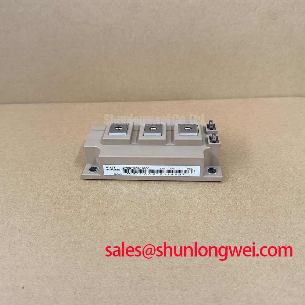
2MBI200VH-170-50 Fuji Electric 1700V 200A IGBT Module
Begin service inspection by isolating the converter, checking the module marking against the maintenance record, and verifying the electrical boundary before any live commissioning. The Fuji Electric 2MBI200VH-170-50 is an IGBT module specified with a 1700 V collector emitter voltage and a 200 A continuous collector current at TC = 100°C. Its published typical collector emitter saturation voltage is 2.55 V at IC = 200 A and Tj = 125°C.
| Parameter | Symbol | Official specification | Conditions |
|---|---|---|---|
| Collector emitter voltage | VCES | 1700 V | Not specified |
| Continuous collector current | IC | 200 A | TC = 100°C |
| Collector emitter saturation voltage | VCE(sat) | 2.55 V typical | IC = 200 A, Tj = 125°C |
| Maximum junction temperature | Tj max | 175°C | Not specified |
| IGBT thermal resistance | Rth(j-c) | 0.120°C/W per device | Per device |
| Turn off time | toff | 1050 ns typical | IC = 200 A, Tj = 150°C |
These values are official specification data, not a substitute for the complete Fuji Electric test conditions, switching waveforms, gate requirements, or mechanical drawing. Engineers evaluating the part for a multi megawatt offshore or onshore wind turbine full scale converter should confirm the original converter topology, terminal arrangement, cooling method, and protection coordination before replacement.
2MBI200VH-170-50 Circuit Protection and Reliability: Calibrating Active Miller Clamp Implementation
High dv/dt switching can couple transient current into the gate loop and create an unintended turn on event in the opposite device. An active Miller clamp may be evaluated where the gate driver topology supports a dedicated low impedance path during the off state. A negative gate bias may also be considered, but the permitted bias range must come from the selected driver and the complete Fuji Electric application documentation rather than from a generic module assumption.
Keep the gate loop compact, place the driver return with the relevant emitter reference, and separate power commutation conductors from sensitive control wiring. The system designer should define clearance and creepage from the converter working voltage, pollution environment, insulation system, and applicable equipment standard. FR 4 is commonly used in power electronics, but the material designation alone does not establish the required insulation performance; reference information on FR 4 flame retardant glass epoxy PCB material should not replace the board manufacturer’s qualification data.
During commissioning, compare gate emitter voltage, collector emitter voltage, and phase current on a known good switching leg. An irregular gate plateau, unexpected gate excursion, or asymmetric turn off waveform may indicate driver reference error, parasitic coupling, probe loading, or an unsuitable clamp implementation. Check the driver supply sequence and fault latch behavior before increasing switching speed. The related 2MBI200UB-120 can be reviewed as a neutral reference for a related device position in a broader system topology, not as an automatic substitute.
Field Diagnostics and Commissioning: Transient Thermal Impedance in 2MBI200VH-170-50 Topologies
The official static thermal value for this device is Rth(j-c) = 0.120°C/W per device. That figure is useful for steady state junction to case assessment, while a pulsed wind converter load requires the manufacturer’s transient thermal impedance curve and the actual pulse profile. If the complete curve is unavailable, do not convert a single steady state value into a claimed peak junction temperature.
For a practical inspection, record case temperature near the specified reference point, phase current, switching frequency, duty pattern, and cooling air or coolant conditions. Apply the thermal impedance curve supplied for the exact device and pulse duration, then combine the resulting junction to case response with the verified case to heatsink and heatsink to ambient path. The calculated peak junction temperature must remain within the official Tj max of 175°C, with the final operating margin established by system testing and the converter duty cycle.
Phase angle control, line frequency ripple, and short overload intervals can produce a thermal pattern that is not visible from average current alone. Inspect the heatsink for dust accumulation, confirm that fans or coolant circuits operate correctly, and examine the interface material for pump out, cracking, contamination, or uneven compression. Maintenance Note: Isolate power before inspection, then monitor contact temperature and verify the cooling airflow during scheduled service.
RC snubbers can reduce switching transients when their values, placement, pulse capability, and losses are validated against measured waveforms. Snubber selection remains a system engineering task. The published typical toff of 1050 ns at IC = 200 A and Tj = 150°C provides a device reference point, but it does not define the converter’s complete commutation loss or thermal response.
Field Diagnostics and Commissioning: Kelvin Emitter Connection in 2MBI200VH-170-50 Topologies
Do not assume a separate Kelvin emitter terminal unless it is confirmed by the module’s original terminal drawing. Where the installed package provides an auxiliary emitter or dedicated driver return, route that control reference separately from the high current emitter path. The purpose is to prevent the voltage developed by common emitter inductance from appearing as a false gate signal.
At the module, inspect terminal pressure, busbar flatness, signs of localized heating, and the condition of the gate return connection. At the driver, measure the gate emitter waveform directly at the module terminals with a suitable differential probe. A waveform that looks clean at the driver board but unstable at the module can indicate return path coupling or excessive interconnect inductance. A discrepancy between parallel switching positions should be investigated through conductor symmetry, connector condition, gate resistance placement, and driver timing.
Designers should verify the module’s actual pinout and auxiliary terminal function from the original Fuji Electric documentation before routing a replacement board. The Fuji Electric Power Semiconductors Portal provides manufacturer product context, while the exact device drawing remains the controlling document for installation.
Reverse recovery behavior of the freewheel diode can affect commutation current, overshoot, and radiated EMI. A softness factor is not included in the official parameter set provided for this product, so engineers should obtain the relevant diode recovery curves and test conditions before using that value in an EMI or loss model. Measure both conducted noise and near field emissions after the gate return and power loop have been corrected; a diode parameter alone cannot establish compliance with CISPR or any complete equipment EMC requirement.
Preventing Spurious Faults: Planar Symmetrical Busbar Geometry for 2MBI200VH-170-50
During turn off, stray inductance and current slew interact to create collector emitter overshoot. The engineering relationship can be considered in the form of the DC link voltage plus the inductive contribution from the commutation loop, with the peak verified directly at the module terminals. The target inductance, snubber capacitance, damping, and busbar geometry must be determined by the system engineer from measured switching conditions; no universal layout number should be treated as an official rating of this module.
Use closely coupled forward and return conductors, minimize the physical area of the commutation loop, and keep parallel phase paths geometrically consistent. Avoid unnecessary vias, long flexible links, and narrow necks near high current terminals. Check the DC link capacitor connection, laminated busbar joints, terminal fasteners, and snubber attachment points as one electrical loop rather than as isolated components.
Commissioning should begin at a controlled switching condition with voltage and current probes positioned to minimize measurement loop area. Compare overshoot across multiple legs, inspect ringing frequency and damping, and confirm that the measured peak remains compatible with the 1700 V VCES rating and the converter’s selected operating margin. If the waveform changes after enclosure assembly, investigate busbar alignment, shield placement, cable routing, and the bonding path.
The related 2MBI200UR-120-01 may be reviewed as a neutral same family reference during application comparison. For broader technology context when assessing alternative switching platforms, see the Wide Bandgap Revolution engineering guide.