
Content last revised on September 10, 2026
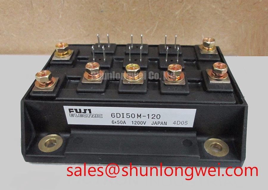
6DI50M-120 Circuit Protection & Reliability: Calibrating Transient Thermal Impedance
Heavy pulsed overload analysis should begin with the actual switching waveform, pulse duration, repetition pattern, case temperature, and cooling arrangement. The official 1200.0 V and 50.0 A ratings are essential identity data, while transient thermal impedance must be taken from the applicable Fuji Electric technical documentation for the precise operating condition. Do not convert the continuous current rating directly into a short pulse limit.
An engineering calculation may use a multi RC junction to case thermal model when the relevant thermal impedance curve and pulse profile are available. The engineer can then estimate junction temperature by combining the case temperature with the transient power response, while checking the result against the device’s documented temperature and switching limits. The calculation remains system dependent because heatsink contact, airflow, thermal interface condition, load power factor, and switching frequency all affect the result.
During field troubleshooting, capture collector emitter voltage, current, gate emitter voltage, and case temperature under the same load condition used by the original drive. Unexpected overshoot or extended current tails may indicate layout inductance, gate resistance variation, insufficient clamping, or a control timing issue. Verify the complete commutation loop and compare the waveform with a known good drive before assigning a single cause.
Assembly Integrity & Layout Architecture: Implementing Galvanic Gate Drive Isolation, Reinforced for 6DI50M-120
The module should be evaluated with the gate driver, isolation barrier, protection circuit, and control reference as one switching system. A reinforced isolation requirement or a common mode transient immunity target must be confirmed from the selected gate driver and system safety documentation; those values are not official specifications of the 6DI50M-120 provided here. Designers should verify creepage, clearance, insulation coordination, and isolation test conditions against the equipment standard and working voltage.
Dead time should be established from measured turn off delay, driver propagation mismatch, temperature, and the switching behavior of the complete bridge. Too little dead time can create cross conduction, while excessive dead time can increase diode conduction and distortion. The gate loop should be compact, with the return path kept close to the drive path. Miller plateau behavior and the effective reverse transfer capacitance should be checked during bench switching tests, particularly when a high dv/dt event produces an unwanted gate voltage excursion.
Active gate clamping can be considered where the driver architecture supports it, but the clamp threshold and response must be selected from measured gate waveforms and the module’s documented gate limits. A high speed semiconductor fuse also requires coordination with the module’s documented short circuit and surge capability. Compare fuse I²t clearing behavior with the fault energy, DC link conditions, wiring inductance, and protection delay instead of treating the fuse rating as an independent guarantee. Fuji Electric’s power semiconductor and IPM reference provides useful manufacturer context for this class of product.
💡 Bench Tip: Keep the module disconnected from the energized DC link during resistance and diode checks, use ESD controls, and record a cold baseline before comparing readings.
6DI50M-120 Circuit Protection & Reliability: Calibrating Thermal Cycling Margins of Internal Braking
When the module is used in a heavy duty variable frequency AC motor drive, the braking path must be reviewed from the complete DC link topology. The 6DI50M-120 product data supplied here does not confirm an internal braking transistor, braking resistor rating, or braking duty cycle. The system integrator should therefore verify whether the original circuit uses this module for switching, rectification, braking, or another topology before approving a replacement.
Deceleration energy depends on motor speed, reflected load inertia, commanded ramp, regeneration path, DC link capacitance, and resistor temperature. An engineering recommendation is to measure the DC link rise during the actual deceleration profile and confirm that the braking switch, resistor, fuse, and enclosure cooling remain within their respective documented limits. Repeated short braking events and occasional long braking events should be evaluated separately because their thermal responses are different.
Inspect the braking loop for loose power connections, damaged insulation, discolored terminals, and abnormal gate signals. If the resistor appears electrically sound but the DC link still rises unexpectedly, verify the braking command, driver supply, switching waveform, and current sensor path. The Fuji Electric PIM reference can help engineers distinguish module family information from application level braking requirements. A neutral comparison may also include 7MBR50SA120-50, subject to terminal, electrical, thermal, and mechanical verification.
Assembly Integrity & Layout Architecture: Implementing Long Motor Lead Reflected Wave Voltage for 6DI50M-120
Long motor cables should be treated as a transmission path rather than an ideal wire. Impedance mismatch can reflect switching energy toward the motor terminals and increase voltage stress at the module output. The actual peak depends on DC link voltage, cable construction, length, switching edge rate, motor impedance, grounding, and termination. Engineers should measure the motor side and inverter side with suitable differential probes before selecting a filter.
A dv/dt filter, output reactor, or sinusoidal filter may be considered when measured voltage edges exceed the motor insulation or drive system limits. The filter must be checked for current capability, resonance, leakage current, thermal loss, grounding behavior, and compatibility with the control algorithm. Minimize stray inductance in the high current commutation loop to reduce overshoot, then verify peak voltage margins during switching tests at the intended load and cable arrangement.
For long lead troubleshooting, inspect cable shield termination, protective earth continuity, output filter connections, and switching frequency settings. Compare phase to phase and phase to earth waveforms, since a problem visible in one measurement may not represent the complete insulation stress. Broader material on switching technology is available in the Wide Bandgap Revolution reference, while selection of this silicon power module should remain anchored to the documented 1200.0 V, 50.0 A, and package requirements.