Content last revised on September 12, 2026
6DI50Z-120 Circuit Protection and Gate Drive Loop Geometry
| Manufacturer | Fuji Electric |
| Model | 6DI50Z-120 |
| Category | IGBT Module |
| Rated voltage | 1200.0 V |
| Rated current | 50.0 A |
| Package | IGBT Module |
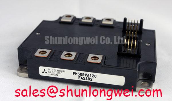
Begin replacement evaluation by checking the nameplate rating, housing condition, terminal alignment, and the cold-state impedance of the corresponding power paths with the equipment isolated. The Fuji Electric 6DI50Z-120 is specified as a 1200.0 V, 50.0 A IGBT Module. These are official product parameters and should be compared with the original inverter welder or medium-frequency induction heating power stage before installation.
Gate-drive wiring requires careful separation between the high-current emitter return and the driver reference path. This is an engineering recommendation because shared copper can introduce emitter mutual coupling, ground movement, and unwanted gate-voltage oscillation during fast switching. Designers should minimize the power commutation loop area, keep the gate loop compact, and verify the actual gate-to-emitter waveform directly at the module terminals. The final layout must be validated against switching overshoot, ringing, and the available DC-link voltage.
When assessing a replacement, compare the terminal arrangement, electrical polarity, mounting pattern, and driver interface with the original equipment documentation. The 7MBR50SA120-50 may be reviewed as a separate same-class reference device, but compatibility must be established from the complete circuit, mechanical drawing, and switching requirements rather than from voltage and current ratings alone.
💡 Pro Tip: Use a symmetrical busbar arrangement and verify turn-off peak voltage with a properly referenced oscilloscope probe during double-pulse or controlled commissioning tests.
Field Diagnostics and Commissioning for 6DI50Z-120 Drive Topologies
Before applying high voltage, confirm driver isolation, gate polarity, supply sequencing, and the return-current path. An optocoupler or digital isolation stage can be suitable only when its insulation rating, common-mode transient immunity, propagation delay, and output behavior match the system requirements. A reinforced isolation barrier above 5 kV and a CMTI capability above 100 kV/µs should be treated as design-verification criteria when required by the selected driver documentation, not as specifications of the 6DI50Z-120 itself.
For phase-angle or pulse-width controlled equipment, observe the relationship between command timing, gate pulses, collector-emitter voltage, and load current. Line-frequency ripple smoothing belongs to the surrounding converter design and should be checked at the DC link under the actual welding or induction-heating load. If a snubber or MOV network is used, select and validate it from measured switching energy, repetitive pulse conditions, leakage behavior, and thermal dissipation. The module’s official ratings do not establish a universal snubber value or MOV selection.
A missing gate pulse, abnormal ringing, or uneven phase current should be investigated through the complete signal path. Check the controller output, isolation barrier, driver supply, gate resistor network, module terminals, and current feedback before assigning a cause. Compare the suspect channel with a known-good channel using the same probe reference and operating conditions.
Fuji Electric’s power semiconductor and IPM module information can provide useful manufacturer-level context, while the original equipment documentation remains the controlling reference for interface and protection settings.
Assembly Integrity and Dynamic Thermal Layout Architecture
Mechanical installation should begin with a clean, flat mounting surface and a review of the equipment manufacturer’s clamping method. A power module’s electrical rating does not define a universal mounting torque, thermal compound thickness, pressure profile, or heatsink flatness requirement. These values are system and assembly dependent, so the integrator should follow the applicable mechanical drawing and verify the result through thermal testing.
For pulsed welding or induction-heating duty, junction temperature should be evaluated with the complete transient thermal path rather than with average current alone. A multi-stage thermal model can represent case, heatsink, and cooling response, but the model must be correlated with measured case temperature, pulse duration, repetition rate, and cooling conditions. The official 50.0 A rating should not be treated as a blanket guarantee for every pulse waveform or overload profile.
Inspect the mounting surface after thermal cycling and look for uneven contact, loosened hardware, discoloration, or changes in thermal resistance. Verify that both electrical and mechanical clearances remain suitable for the equipment’s working voltage. If the design uses a pressed interface or spring-loaded clamping system, pressure calibration and parallel loading should be verified according to the original assembly specification.
The required ITSM capability, short-pulse overload window, and junction-temperature recovery behavior must be confirmed from the applicable Fuji Electric documentation for the exact device revision. The Fuji Electric power semiconductor portal is a suitable manufacturer resource for product-family documentation.
Fault-Clearing Dynamics and Desaturation Protection
Short-circuit protection should be coordinated across the gate driver, desaturation or current-sensing circuit, controller interlock, and semiconductor fuse. Type I or Type II protection terminology can describe different detection and shutdown strategies, so the selected driver documentation must define the actual response time and blanking behavior. A sub-10 µs clearing target should be treated as a system validation objective only where it is supported by the driver, module, and application documentation.
Two-stage soft turn-off may reduce the rate of current interruption and help manage inductive overvoltage, but its timing and gate-current profile must be tested with the real busbar, load, snubber, and DC-link conditions. Verify the peak collector-emitter voltage during fault interruption and confirm that the measured waveform remains within the documented device limits. Do not infer short-circuit withstand capability from the 1200.0 V voltage rating alone.
Fast semiconductor fuses should be coordinated using their documented I²t characteristics and the equipment’s available fault energy. The fuse, gate shutdown circuit, MOV network, and mechanical enclosure should be assessed as one protection system. For negative off-bias operation, designers can consult Evolution of Negative Off-Bias Gate Drive Circuits when evaluating Miller-effect control and common-mode ground-bounce behavior. Any selected bias voltage remains a driver and system-design decision that requires bench verification.