Content last revised on October 15, 2026
PM50RVA120 Operational Boundaries: Evaluating Main Terminal Pinout Mechanical Alignment Limits
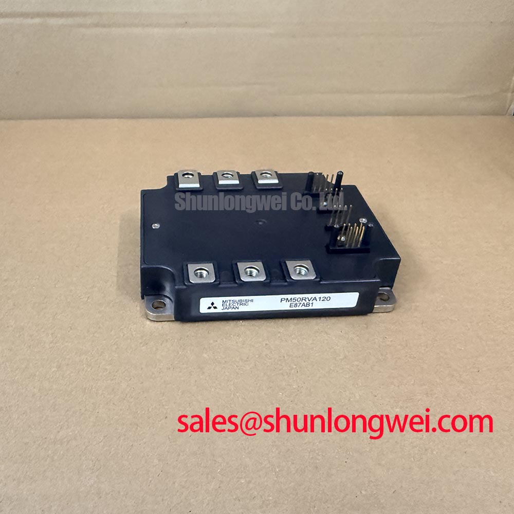
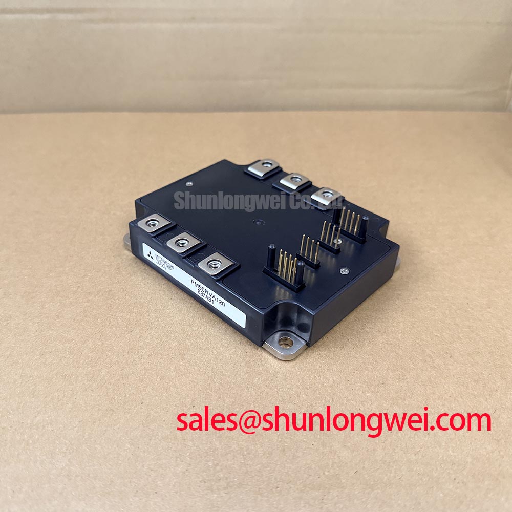
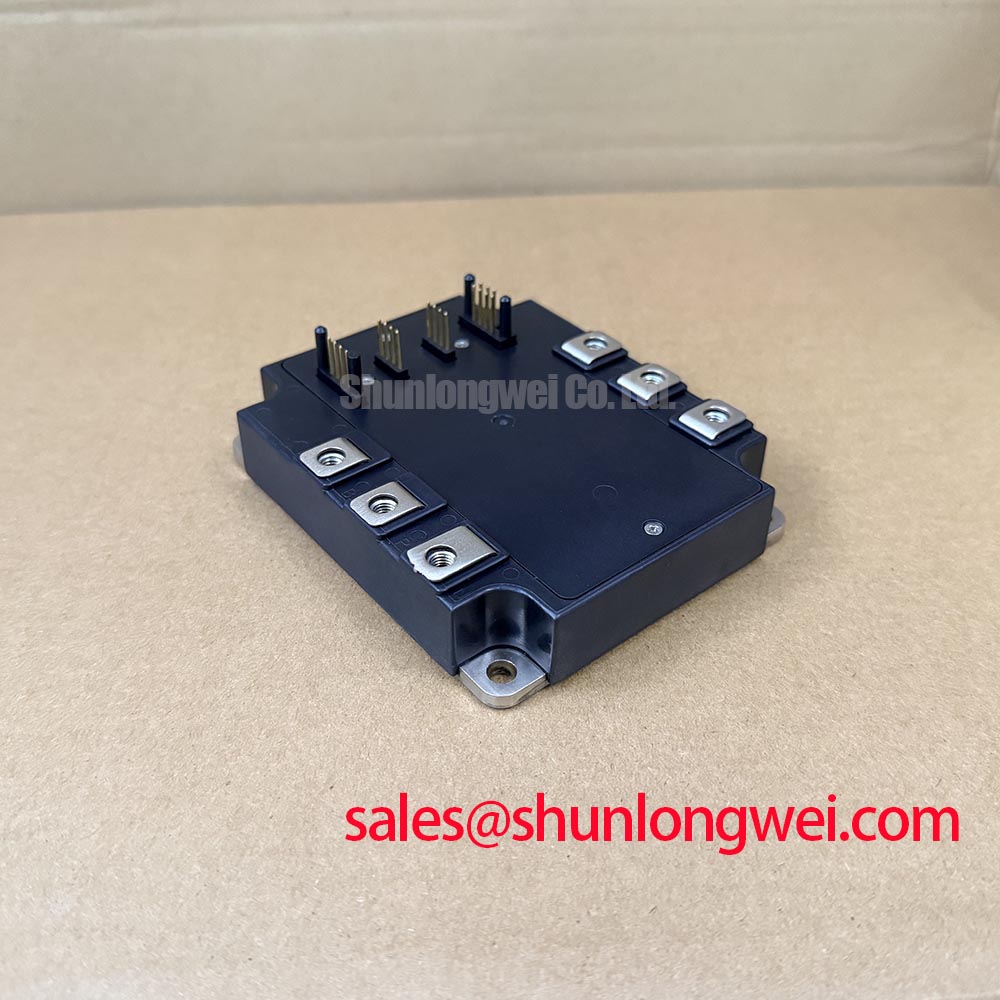
Mechanical alignment at the main terminals determines whether electrical pressure is transferred cleanly through the intended contact surfaces or converted into stress on the internal copper connections. Before installation, place the replacement module on the heatsink without compound and check that every power terminal sits naturally against the busbar or cable lug. A terminal that requires lateral force from the busbar is not correctly aligned, even when the screw appears to engage normally.
Inspect the thread engagement depth with the busbar held in its final position. The screw should enter without cross-threading, and the washer should remain centered on the lug rather than touching molded insulation. A tilted lug can create uneven contact pressure and may loosen during thermal cycling. The correct mechanical sequence is to align the module, position the busbar, engage the fasteners by hand, and only then apply the installation torque specified by the relevant screw, washer, and assembly documentation.
Field Alert: Never use the terminal screw to pull a misaligned busbar into position, because the resulting levering force can transfer directly into the module terminal structure.
Clearance around the power terminals should allow the cable or laminated busbar to remain stationary while the module expands and contracts with temperature. Avoid routing a heavy cable so that its weight, bend radius, or cable tie tension loads the terminal sideways. In a heavy duty variable frequency AC motor drive, vibration from contactors, cooling fans, and motor conductors can expose a mechanically marginal connection even when the first energization appears normal.
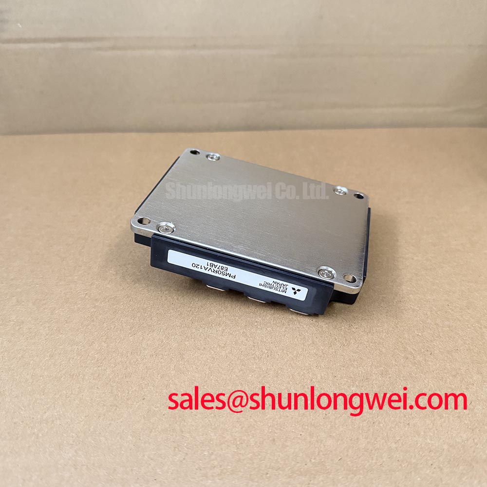
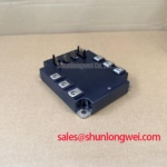
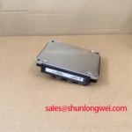
During a field replacement, compare the old and new mounting holes, terminal height, washer position, and busbar entry angle. The package is identified here as a Mitsubishi IPM Module, but physical similarity alone does not establish interchangeability. The mounting pattern, terminal polarity, auxiliary control connections, protective functions, and thermal interface must match the equipment documentation.
For a neutral cross reference, engineers may review CM2500DY 24S as a separate Mitsubishi Electric reference product. It should be treated as a comparison point only. A different current class, internal topology, terminal arrangement, or control interface can make direct substitution unsuitable even when the package appears similar.
| Evaluation item | PM50RVA120 | Replacement review requirement |
|---|---|---|
| Manufacturer | Mitsubishi Electric | Confirm the equipment documentation and original module marking |
| Product category | IPM Module | Match power and control terminal functions |
| Rated voltage | 1200.0 V | Compare the complete switching and DC link conditions |
| Rated current | 50.0 A | Assess load profile, cooling, overload, and switching conditions |
| Mechanical interface | Module package | Check hole pattern, terminal height, insulation clearance, and heatsink contact |
After fastening, check that the module base remains fully supported and that no corner is lifted by excess thermal compound or a distorted heatsink. The thermal interface should be continuous and uniform, while the clamping method should follow the assembly specification for the actual hardware. A cold mechanical inspection is often more useful than immediately applying full DC-link voltage to a drive that has just received a replacement power module.
PM50RVA120 Circuit Protection & Reliability: Calibrating Auxiliary Emitter Pinout Cold-Check
The auxiliary emitter return must be treated as a dedicated driver reference rather than casually bonded to the main load return at an arbitrary point. In a high-current switching path, the main emitter conductor carries commutation current and develops parasitic voltage during fast transitions. The gate driver reference should follow the module pin definition and the original control-board topology so that this voltage is not interpreted as an unintended gate signal.
Begin the cold check by isolating the gate driver, removing external gate resistors where the service procedure permits, and identifying the main emitter and auxiliary emitter from the original module documentation. Do not infer pin identity from physical proximity. Measure continuity through the complete board path, inspect solder joints and connector crimps, and compare the return routing with a known-good channel when the drive contains multiple identical legs.
A disagreement between the main emitter return and the auxiliary driver return can appear as false gate activity, irregular turn-off, or unexplained current imbalance. These symptoms do not establish a single failed component. Check the driver supply, gate resistor network, isolation barrier, connector seating, and reference routing together. The oscilloscope probe reference must be selected carefully; an incorrectly referenced probe can create a misleading waveform and may introduce a hazardous current path.
The freewheeling path also requires attention. Reverse recovery behavior in the external diode or paired switching path can produce a current impulse that couples into the gate loop and control ground. A snubber can reduce ringing when its placement, impedance, pulse capability, and thermal behavior are validated against measured waveforms. Snubber selection is an engineering recommendation determined by the complete commutation loop, not a fixed PM50RVA120 parameter.
For a drive that includes a front-end rectifier or another high-power conversion stage, the surrounding topology should be examined rather than treating the IPM as an isolated repair. The CM100MXA 24S can be reviewed as a separate peripheral reference in equipment architecture analysis. Its presence does not establish a required pairing with the PM50RVA120, and the system engineer must confirm voltage path, control coordination, protection timing, and thermal interaction.
Gate turn-off behavior should be checked during controlled low-energy testing before normal motor operation. Look for clean separation between the command signal and the emitter reference, consistent turn-on and turn-off timing among phases, and absence of repetitive ringing that approaches the driver’s functional limits. When the signal becomes unstable only after the power stage is energized, investigate common-mode coupling, auxiliary emitter routing, diode recovery, and busbar geometry together rather than assigning the symptom to the module alone.
Industrial equipment such as a heavy-duty variable frequency AC motor drive may also contain braking choppers, regenerative energy paths, or large braking resistors. These circuits can return transient energy to the DC link and change the stress applied to the IPM. Designers should verify the braking control sequence, DC-link protection response, and resistor thermal duty during commissioning. The PM50RVA120 rating does not by itself define the permissible regenerative operating profile.
For structured troubleshooting references covering terminal checks, switching faults, and reliability-oriented inspection, consult the Field Engineer’s Handbook. Device-level observations should be recorded with the actual drive state, load condition, temperature, and measurement location so that later comparisons remain meaningful.
Benchtop Waveform Tuning: Mitigating Stress via DC-Link Capacitance Bank Layout and Low-ESR on PM50RVA120
Place the local DC-link capacitance so that the commutation loop remains compact and geometrically balanced around the switching path. The practical objective is to minimize parasitic loop inductance and reduce the voltage overshoot produced when current changes rapidly. In engineering terms, the peak voltage rises with both stray inductance and current slew rate, so the measured switching waveform must be compared with the module’s rated voltage and the system’s protection margin.
Low-ESR capacitors may reduce high-frequency impedance, but the capacitor type alone does not solve a poorly arranged busbar. Long opposing conductors, uneven phase geometry, and remote capacitor banks can add inductive voltage that appears only during switching. Use a symmetrical laminated or closely coupled conductor arrangement where practical, keep the high-current path physically short, and prevent the gate-control wiring from running parallel to the strongest commutation field.
Bench testing should begin with controlled DC-link energy and current, using differential voltage measurement and a current probe suitable for the expected transient. Capture turn-on, turn-off, diode recovery, and braking events separately. When ringing is present, vary one physical or electrical condition at a time: probe placement, gate resistance, snubber location, capacitor position, or load current. This separates measurement artifacts from actual power-loop behavior.
Snubber capacitor sizing must be based on measured overshoot, ringing frequency, pulse energy, and component temperature. The required capacitance and damping resistance are system-determined values, not published PM50RVA120 specifications. The same principle applies to gate damping and any negative turn-off bias. Designers should verify the driver’s permitted gate-emitter range, common-mode transient behavior, and fault response from the applicable control documentation before changing the original circuit.
The Mitsubishi Electric semiconductor resource on SiC Power Modules and SBDs provides broader manufacturer technical context for modern power semiconductor switching, but it should not be read as a PM50RVA120-specific operating specification. The PM50RVA120 remains identified by the supplied official values of 1200.0 V, 50.0 A, and Mitsubishi IPM module construction.
When the waveform passes the initial bench check, repeat the test at the intended cooling condition and with the actual gate-driver harness, DC-link assembly, braking path, and motor-side cabling. Confirm that the measured peak voltage, current sharing, gate-emitter behavior, and heatsink temperature remain acceptable throughout the operating sequence. Only then should the repaired drive proceed to staged load testing.